- Basic Electronics - Materials
- Basic Electronics - Energy Bands
- Basic Electronics - Semiconductors
- Basic Electronics - Hall Effect
- Resistors
- Basic Electronics - Resistors
- Circuit Connections in Resistors
- Non-linear Resistors
- Basic Electronics - Linear Resistors
- Basic Electronics - Fixed Resistors
- Capacitors
- Basic Electronics - Capacitors
- Circuit Connections in Capacitors
- Variable Capacitors
- Basic Electronics - Fixed Capacitors
- Polarized Capacitors
- Inductors
- Basic Electronics - Inductors
- Basic Electronics - Inductance
- Circuit Connections in Inductors
- Types of Inductors
- Basic Electronics - RF Inductors
- Transformers
- Basic Electronics - Transformers
- Types of Transformers
- Transformers based on Usage
- Transformer Efficiency
- Diodes
- Basic Electronics - Diodes
- Basic Electronics - Junction Diodes
- Special Purpose Diodes
- Optoelectronic Diodes
- Transistors
- Basic Electronics - Transistors
- Transistor Configurations
- Transistor Regions of Operation
- Transistor Load Line Analysis
- Types of Transistors
- Basic Electronics - JFET
- Basic Electronics - MOSFET
- Basic Electronics Useful Resources
- Basic Electronics - Quick Guide
- Basic Electronics - Useful Resources
- Basic Electronics - Discussion
Transistor Load Line Analysis
Till now we have discussed different regions of operation for a transistor. But among all these regions, we have found that the transistor operates well in active region and hence it is also called as linear region. The outputs of the transistor are the collector current and collector voltages.
Output Characteristics
When the output characteristics of a transistor are considered, the curve looks as below for different input values.
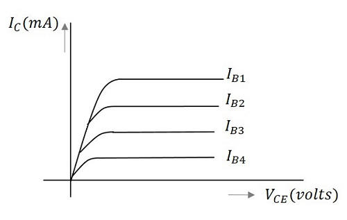
In the above figure, the output characteristics are drawn between collector current IC and collector voltage VCE for different values of base current IB. These are considered here for different input values to obtain different output curves.
Operating point
When a value for the maximum possible collector current is considered, that point will be present on the Y-axis, which is nothing but the saturation point. As well, when a value for the maximum possible collector emitter voltage is considered, that point will be present on the X-axis, which is the cutoff point.
When a line is drawn joining these two points, such a line can be called as Load line. This is called so as it symbolizes the output at the load. This line, when drawn over the output characteristic curve, makes contact at a point called as Operating point.
This operating point is also called as quiescent point or simply Q-point. There can be many such intersecting points, but the Q-point is selected in such a way that irrespective of AC signal swing, the transistor remains in active region. This can be better understood through the figure below.
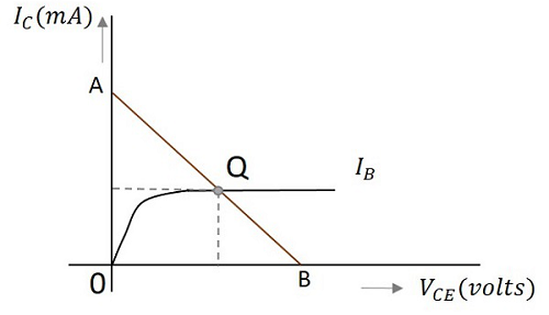
The load line has to be drawn in order to obtain the Q-point. A transistor acts as a good amplifier when it is in active region and when it is made to operate at Q-point, faithful amplification is achieved.
Faithful amplification is the process of obtaining complete portions of input signal by increasing the signal strength. This is done when AC signal is applied at its input. This is discussed in AMPLIFIERS tutorial.
DC Load line
When the transistor is given the bias and no signal is applied at its input, the load line drawn at such condition, can be understood as DC condition. Here there will be no amplification as the signal is absent. The circuit will be as shown below.
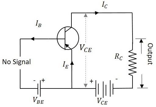
The value of collector emitter voltage at any given time will be
$$V_{CE}\:=\:V_{CC}\:-\:I_{C}R_{C}$$
As VCC and RC are fixed values, the above one is a first degree equation and hence will be a straight line on the output characteristics. This line is called as D.C. Load line. The figure below shows the DC load line.
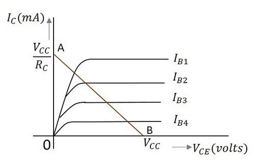
To obtain the load line, the two end points of the straight line are to be determined. Let those two points be A and B.
To obtain A
When collector emitter voltage VCE = 0, the collector current is maximum and is equal to VCC/RC. This gives the maximum value of VCE. This is shown as
$$V_{CE}\:=\:V_{CC}\:-\:I_{C}R_{C}$$
$$0\:=\:V_{CC}\:-\:I_{C}R_{C}$$
$$I_{C}\:=\:\frac{V_{CC}}{R_{C}}$$
This gives the point A (OA = VCC/RC) on collector current axis, shown in the above figure.
To obtain B
When the collector current IC = 0, then collector emitter voltage is maximum and will be equal to the VCC. This gives the maximum value of IC. This is shown as
$$V_{CE}\:=\:V_{CC}\:-\:I_{C}R_{C}$$
$$=\:V_{CC}$$
(As IC = 0)
This gives the point B, which means (OB = VCC) on the collector emitter voltage axis shown in the above figure.
Hence we got both the saturation and cutoff point determined and learnt that the load line is a straight line. So, a DC load line can be drawn.
The importance of this operating point is further understood when an AC signal is given at the input. This will be discussed in AMPLIFIERS tutorial.
