- Basic Electronics - Materials
- Basic Electronics - Energy Bands
- Basic Electronics - Semiconductors
- Basic Electronics - Hall Effect
- Resistors
- Basic Electronics - Resistors
- Circuit Connections in Resistors
- Non-linear Resistors
- Basic Electronics - Linear Resistors
- Basic Electronics - Fixed Resistors
- Capacitors
- Basic Electronics - Capacitors
- Circuit Connections in Capacitors
- Variable Capacitors
- Basic Electronics - Fixed Capacitors
- Polarized Capacitors
- Inductors
- Basic Electronics - Inductors
- Basic Electronics - Inductance
- Circuit Connections in Inductors
- Types of Inductors
- Basic Electronics - RF Inductors
- Transformers
- Basic Electronics - Transformers
- Types of Transformers
- Transformers based on Usage
- Transformer Efficiency
- Diodes
- Basic Electronics - Diodes
- Basic Electronics - Junction Diodes
- Special Purpose Diodes
- Optoelectronic Diodes
- Transistors
- Basic Electronics - Transistors
- Transistor Configurations
- Transistor Regions of Operation
- Transistor Load Line Analysis
- Types of Transistors
- Basic Electronics - JFET
- Basic Electronics - MOSFET
- Basic Electronics Useful Resources
- Basic Electronics - Quick Guide
- Basic Electronics - Useful Resources
- Basic Electronics - Discussion
Basic Electronics - Quick Guide
Basic Electronics - Materials
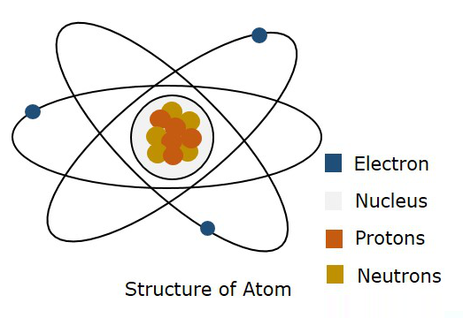
Matter is made up of molecules which consists of atoms. According to Bohrs theory, the atom consists of positively charged nucleus and a number of negatively charged electrons which revolve round the nucleus in various orbits. When an electron is raised from a lower state to a higher state, it is said to be excited. While exciting, if the electron is completely removed from the nucleus, the atom is said to be ionized. So, the process of raising the atom from normal state to this ionized state is called as ionization.
The following figure shows the structure of an atom.
According to Bohrs model, an electron is said to be moved in a particular Orbit, whereas according to quantum mechanics, an electron is said to be somewhere in free space of the atom, called as Orbital. This theory of quantum mechanics was proven to be right. Hence, a three dimensional boundary where an electron is probable to found is called as Atomic Orbital.
Quantum Numbers
Each orbital, where an electron moves, differs in its energy and shape. The energy levels of orbitals can be represented using discrete set of integrals and half-integrals known as quantum numbers. There are four quantum numbers used to define a wave function.
Principal Quantum number
The first quantum number that describes an electron is the Principal quantum number. Its symbol is n. It specifies the size or order (energy level) of the number. As the value of n increases, the average distance from electron to nucleus also increases, as well, the energy of the electron also increases. The main energy level can be understood as a shell.
Angular Momentum Quantum number
This quantum number has l as its symbol. This l indicates the shape of the orbital. It ranges from 0 to n-1.
l = 0, 1, 2 n-1
For the first shell, n = 1.
i.e., for n-1, l = 0 is the only possible value of l as n = 1.
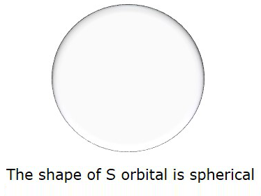
So, when l = 0, it is called as S orbital. The shape of S is spherical. The following figure represents the shape of S.
If n = 2, then l = 0, 1 as these are the two possible values for n = 2.
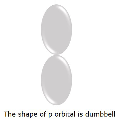
We know that it is S orbital for l = 0, but if l = 1, it is P orbital.
The P orbital where the electrons are more likely to find is in dumbbell shape. It is shown in the following figure.
Magnetic Quantum number
This quantum number is denoted by ml which represents the orientation of an orbital around the nucleus. The values of ml depend on l.
$$m_{l}= \int (-l\:\:to\:+l)$$
For l = 0, ml = 0 this represents S orbital.
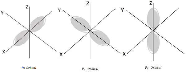
For l = 1, ml = -1, 0, +1 these are the three possible values and this represents P orbital.
Hence we have three P orbitals as shown in the following figure.
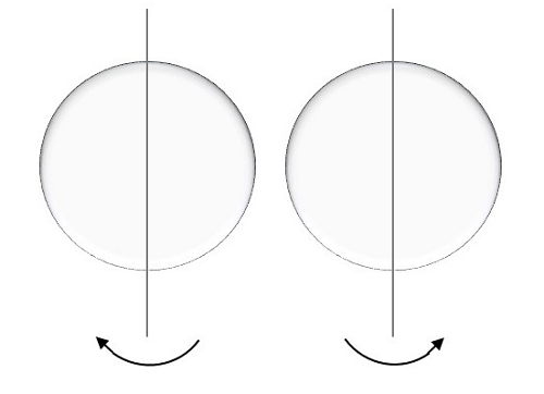
Spin Quantum number
This is represented by ms and the electron here, spins on the axis. The movement of the spinning of electron could be either clockwise or anti-clockwise as shown here under.
The possible values for this spin quantum number will be like,
$$m_{s}= +\frac{1}{2}\:\:up$$
For a movement called spin up, the result is positive half.
$$m_{s}= -\frac{1}{2}\:\:down$$
For a movement called spin down, the result is negative half.
These are the four quantum numbers.
Pauli Exclusion Principle
According to Pauli Exclusion Principle, no two electrons in an atom can have the same set of four identical quantum numbers. It means, if any two electrons have same values of n, s, ml (as we just discussed above) then the l value would definitely be different in them. Hence, no two electrons will have same energy.
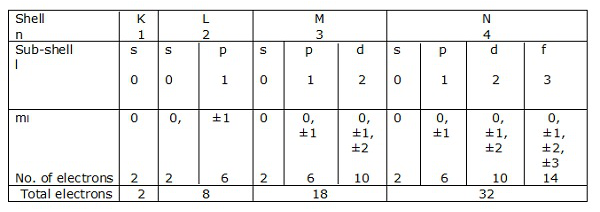
Electronic shells
If n = 1 is a shell, then l = 0 is a sub-shell.
Likewise, n = 2 is a shell, and l = 0, 1 is a sub-shell.
Shells of electrons corresponding to n = 1, 2, 3.. are represented by K, L, M, N respectively. The sub-shells or the orbitals corresponding to l = 0, 1, 2, 3 etc. are denoted by s, p, d, f etc. respectively.
Let us have a look at the electronic configurations of carbon, silicon and germanium (Group IV A).
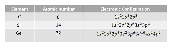
It is observed that the outermost p sub-shell in each case contains only two electrons. But the possible number of electrons is six. Hence, there are four valence electrons in each outer most shell. So, each electron in an atom has specific energy. The atomic arrangement inside the molecules in any type of substance is almost like this. But the spacing between the atoms differ from material to material.
Basic Electronics - Energy Bands
In gaseous substances, the arrangement of molecules is not close. In liquids, the molecular arrangement is moderate. But, in solids, the molecules are so closely arranged, that the electrons in the atoms of molecules tend to move into the orbitals of neighboring atoms. Hence the electron orbitals overlap when the atoms come together.
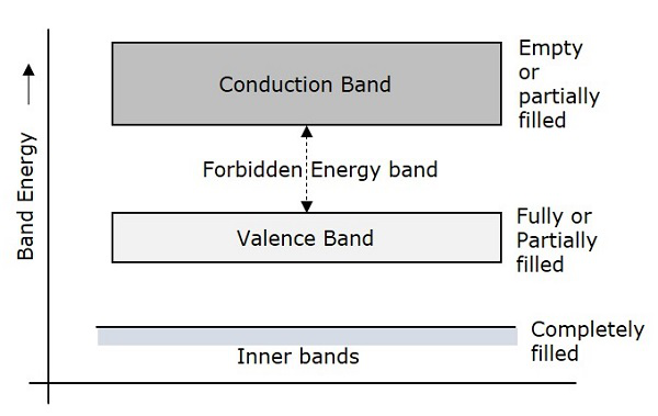
Due to the intermixing of atoms in solids, instead of single energy levels, there will be bands of energy levels formed. These set of energy levels, which are closely packed are called as Energy bands.
Valance Band
The electrons move in the atoms in certain energy levels but the energy of the electrons in the innermost shell is higher than the outermost shell electrons. The electrons that are present in the outermost shell are called as Valance Electrons.
These valance electrons, containing a series of energy levels, form an energy band which is called as Valence Band. The valence band is the band having the highest occupied energy.
Conduction Band
The valence electrons are so loosely attached to the nucleus that even at room temperature, few of the valence electrons leave the band to be free. These are called as free electrons as they tend to move towards the neighboring atoms.
These free electrons are the ones which conduct the current in a conductor and hence called as Conduction Electrons. The band which contains conduction electrons is called as Conduction Band. The conduction band is the band having the lowest occupied energy.
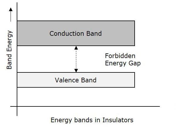
Forbidden gap
The gap between valence band and conduction band is called as forbidden energy gap. As the name implies, this band is the forbidden one without energy. Hence no electron stays in this band. The valence electrons, while going to the conduction band, pass through this.
The forbidden energy gap if greater, means that the valence band electrons are tightly bound to the nucleus. Now, in order to push the electrons out of the valence band, some external energy is required, which would be equal to the forbidden energy gap.
The following figure shows the valance band, conduction band, and the forbidden gap.
Depending upon the size of the forbidden gap, the Insulators, the Semiconductors and the Conductors are formed.
Insulators
Insulators are such materials in which the conduction cannot take place, due to the large forbidden gap. Examples: Wood, Rubber. The structure of energy bands in Insulators is as shown in the following figure.
Characteristics
The following are the characteristics of Insulators.
The Forbidden energy gap is very large.
Valance band electrons are bound tightly to atoms.
The value of forbidden energy gap for an insulator will be of 10eV.
For some insulators, as the temperature increases, they might show some conduction.
The resistivity of an insulator will be in the order of 107 ohm-meter.
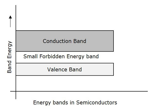
Semiconductors
Semiconductors are such materials in which the forbidden energy gap is small and the conduction takes place if some external energy is applied. Examples: Silicon, Germanium. The following figure shows the structure of energy bands in semiconductors.
Characteristics
The following are the characteristics of Semiconductors.
The Forbidden energy gap is very small.
The forbidden gap for Ge is 0.7eV whereas for Si is 1.1eV.
A Semiconductor actually is neither an insulator, nor a good conductor.
As the temperature increases, the conductivity of a semiconductor increases.
The conductivity of a semiconductor will be in the order of 102 mho-meter.
Conductors
Conductors are such materials in which the forbidden energy gap disappears as the valence band and conduction band become very close that they overlap. Examples: Copper, Aluminum. The following figure shows the structure of energy bands in conductors.
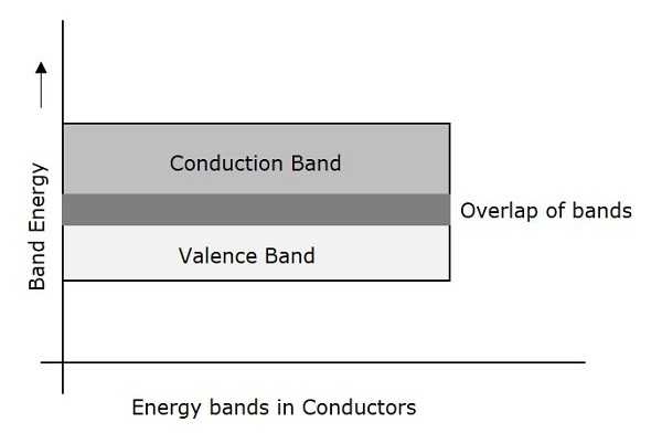
Characteristics
The following are the characteristics of Conductors.
There exists no forbidden gap in a conductor.
The valance band and the conduction band gets overlapped.
The free electrons available for conduction are plenty.
A slight increase in voltage, increases the conduction.
There is no concept of hole formation, as a continuous flow of electrons contribute the current.
Important Terms
There is a necessity to discuss a few important terms here before we move on to subsequent chapters.
Current
It is simply the flow of electrons. A continuous flow of electrons or charged particles, can be termed as Current. It is indicated by I or i. It is measured in Amperes. This can be alternating current AC or direct current DC.
Voltage
It is the potential difference. When there occurs a difference in potentialities, between two points, there is said to be a voltage difference, measured between those two points. It is indicated by V. It is measured in Volts.
Resistance
It is the property of opposing the flow of electrons. The possession of this property can be termed as resistivity. This will be discussed later in detail.
Ohms Law
With the terms discussed above, we have a standard law, which is very crucial for the behavior of all the electronic components, called as Ohms Law. This states the relation between current and voltage in an ideal conductor.
According to Ohms law, the potential difference across an ideal conductor is proportional to the current through it.
$$V\:\alpha\:\:I$$
An ideal conductor has no resistance. But in practice, every conductor has some resistance in it. As the resistance increases, the potential drop also increases and hence the voltage increases.
Hence the voltage is directly proportional to the resistance it offers.
$$V\:\alpha\:\:R$$
$$V = IR $$
But the current is inversely proportional to the resistance.
$$V\:\alpha\:\:I\:\alpha\:\:\frac{1}{R}$$
$$I = V/R $$
Hence, in practice, an Ohms law can be stated as −
According to Ohms law, the current flowing through a conductor is proportional to the potential difference across it, and is inversely proportional to the resistance it offers.
This law is helpful in determining the values of unknown parameters among the three which help to analyze a circuit.
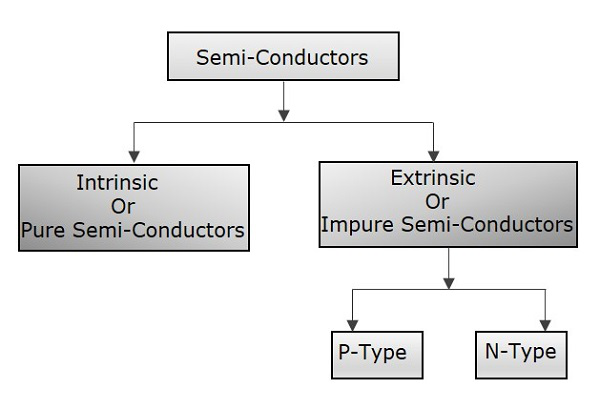
Basic Electronics - Semiconductors
A semiconductor is a substance whose resistivity lies between the conductors and insulators. The property of resistivity is not the only one that decides a material as a semiconductor, but it has few properties as follows.
Semiconductors have the resistivity which is less than insulators and more than conductors.
Semiconductors have negative temperature co-efficient. The resistance in semiconductors, increases with the decrease in temperature and vice versa.
The Conducting properties of a Semiconductor changes, when a suitable metallic impurity is added to it, which is a very important property.
Semiconductor devices are extensively used in the field of electronics. The transistor has replaced the bulky vacuum tubes, from which the size and cost of the devices got decreased and this revolution has kept on increasing its pace leading to the new inventions like integrated electronics. The following illustration shows the classification of semiconductors.
Conduction in Semiconductors
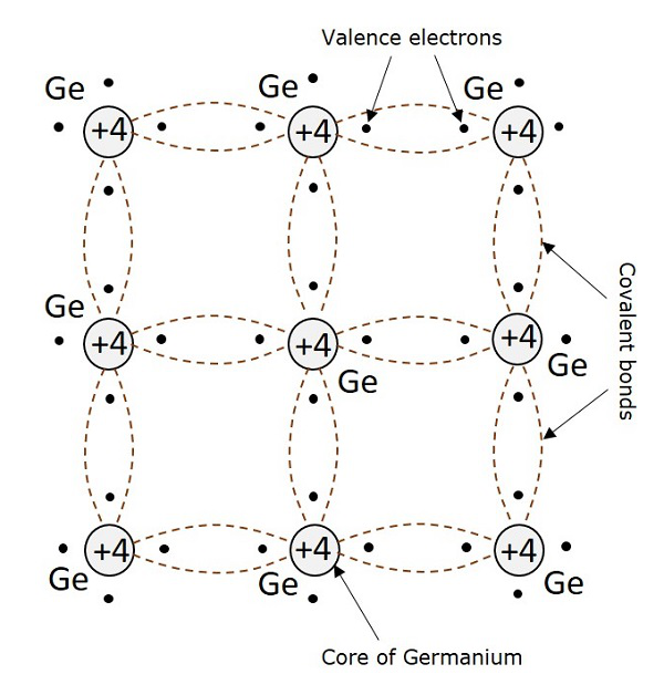
After having some knowledge on the electrons, we came to know that the outermost shell has the valence electrons which are loosely attached to the nucleus. Such an atom, having valence electrons when brought close to the other atom, the valence electrons of both these atoms combine to form Electron pairs. This bonding is not so very strong and hence it is a Covalent bond.
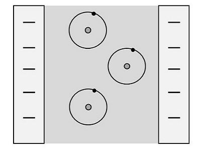
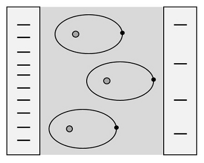
For example, a germanium atom has 32 electrons. 2 electrons in first orbit, 8 in second orbit, 18 in third orbit, while 4 in last orbit. These 4 electrons are valence electrons of germanium atom. These electrons tend to combine with valence electrons of adjoining atoms, to form the electron pairs, as shown in the following figure.
Creation of Hole
Due to the thermal energy supplied to the crystal, some electrons tend to move out of their place and break the covalent bonds. These broken covalent bonds, result in free electrons which wander randomly. But the moved away electrons creates an empty space or valence behind, which is called as a hole.
This hole which represents a missing electron can be considered as a unit positive charge while the electron is considered as a unit negative charge. The liberated electrons move randomly but when some external electric field is applied, these electrons move in opposite direction to the applied field. But the holes created due to absence of electrons, move in the direction of applied field.
Hole Current
It is already understood that when a covalent bond is broken, a hole is created. Actually, there is a strong tendency of semiconductor crystal to form a covalent bond. So, a hole doesnt tend to exist in a crystal. This can be better understood by the following figure, showing a semiconductor crystal lattice.
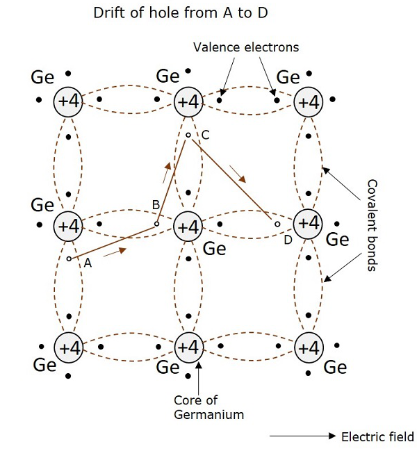
An electron, when gets shifted from a place A, a hole is formed. Due to the tendency for the formation of covalent bond, an electron from B gets shifted to A. Now, again to balance the covalent bond at B, an electron gets shifted from C to B. This continues to build a path. This movement of hole in the absence of an applied field is random. But when electric field is applied, the hole drifts along the applied field, which constitutes the hole current. This is called as hole current but not electron current because, the movement of holes contribute the current flow.
Electrons and holes while in random motion, may encounter with each other, to form pairs. This recombination results in the release of heat, which breaks another covalent bond. When the temperature increases, the rate of generation of electrons and holes increase, thus rate of recombination increases, which results in the increase of densities of electrons and holes. As a result, conductivity of semiconductor increases and resistivity decreases, which means the negative temperature coefficient.
Intrinsic Semiconductors
A Semiconductor in its extremely pure form is said to be an intrinsic semiconductor. The properties of this pure semiconductor are as follows −
- The electrons and holes are solely created by thermal excitation.
- The number of free electrons is equal to the number of holes.
- The conduction capability is small at room temperature.
In order to increase the conduction capability of intrinsic semiconductor, it is better to add some impurities. This process of adding impurities is called as Doping. Now, this doped intrinsic semiconductor is called as an Extrinsic Semiconductor.
Doping
The process of adding impurities to the semiconductor materials is termed as doping. The impurities added, are generally pentavalent and trivalent impurities.
Pentavalent Impurities
The pentavalent impurities are the ones which has five valence electrons in the outer most orbit. Example: Bismuth, Antimony, Arsenic, Phosphorus
The pentavalent atom is called as a donor atom because it donates one electron to the conduction band of pure semiconductor atom.
Trivalent Impurities
The trivalent impurities are the ones which has three valence electrons in the outer most orbit. Example: Gallium, Indium, Aluminum, Boron
The trivalent atom is called as an acceptor atom because it accepts one electron from the semiconductor atom.
Extrinsic Semiconductor
An impure semiconductor, which is formed by doping a pure semiconductor is called as an extrinsic semiconductor. There are two types of extrinsic semiconductors depending upon the type of impurity added. They are N-type extrinsic semiconductor and P-Type extrinsic semiconductor.
N-Type Extrinsic Semiconductor
A small amount of pentavalent impurity is added to a pure semiconductor to result in Ntype extrinsic semiconductor. The added impurity has 5 valence electrons.
For example, if Arsenic atom is added to the germanium atom, four of the valence electrons get attached with the Ge atoms while one electron remains as a free electron. This is as shown in the following figure.
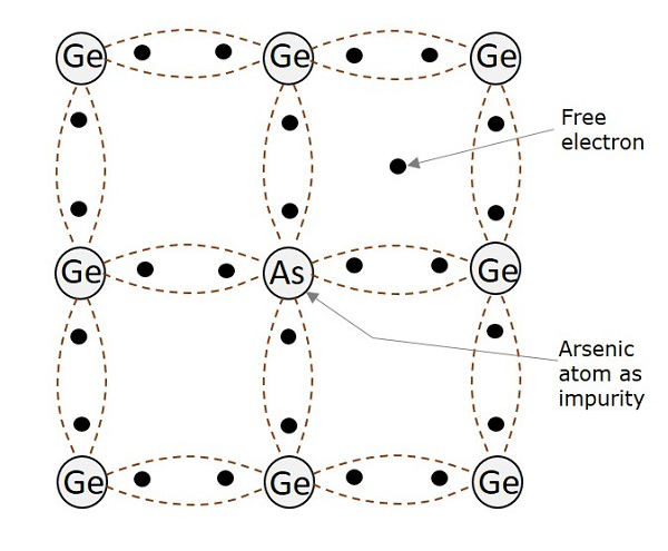
All of these free electrons constitute electron current. Hence, the impurity when added to pure semiconductor, provides electrons for conduction.
In N-type extrinsic semiconductor, as the conduction takes place through electrons, the electrons are majority carriers and the holes are minority carriers.
As there is no addition of positive or negative charges, the electrons are electrically neutral.
When an electric field is applied to an N-type semiconductor, to which a pentavalent impurity is added, the free electrons travel towards positive electrode. This is called as negative or N-type conductivity.
P-Type Extrinsic Semiconductor
A small amount of trivalent impurity is added to a pure semiconductor to result in P-type extrinsic semiconductor. The added impurity has 3 valence electrons. For example, if Boron atom is added to the germanium atom, three of the valence electrons get attached with the Ge atoms, to form three covalent bonds. But, one more electron in germanium remains without forming any bond. As there is no electron in boron remaining to form a covalent bond, the space is treated as a hole. This is as shown in the following figure.
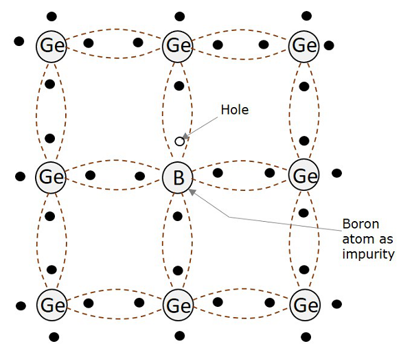
The boron impurity when added in a small amount, provides a number of holes which helps in the conduction. All of these holes constitute hole current.
In P-type extrinsic semiconductor, as the conduction takes place through holes, the holes are majority carriers while the electrons are minority carriers.
The impurity added here provides holes which are called as acceptors, because they accept electrons from the germanium atoms.
As the number of mobile holes remains equal to the number of acceptors, the Ptype semiconductor remains electrically neutral.
When an electric field is applied to a P-type semiconductor, to which a trivalent impurity is added, the holes travel towards negative electrode, but with a slow pace than electrons. This is called as P-type conductivity.
In this P-type conductivity, the valence electrons move from one covalent bond to another, unlike N-type.
Why Silicon is Preferred in Semiconductors?
Among the semiconductor materials like germanium and silicon, the extensively used material for manufacturing various electronic components is Silicon (Si). Silicon is preferred over germanium for many reasons such as −
The energy band gap is 0.7ev, whereas it is 0.2ev for germanium.
The thermal pair generation is smaller.
The formation of SiO2 layer is easy for silicon, which helps in the manufacture of many components along with integration technology.
Si is easily found in nature than Ge.
Noise is less in components made up of Si than in Ge.
Hence, Silicon is used in the manufacture of many electronic components, which are used to make different circuits for various purposes. These components have individual properties and particular uses.
The main electronic components include Resistors, variable resistors, Capacitors, variable capacitors, Inductors, diodes, Tunnel diodes, Varactor diodes, Transistors, BJTs, UJTs, FETs, MOSFETs, LDR, LED, Solar cells, Thermistor, Varistor, Transformer, switches, relays, etc.
Basic Electronics - Hall Effect
Hall Effect was named after Edwin Hall, its discoverer. This is somewhat similar to Flemings right hand rule. When a current carrying conductor I is placed in a transverse magnetic field B, an electric field E is induced in the conductor perpendicular to both I and B. This phenomenon is called as Hall Effect.
Explanation
When a current carrying conductor is placed in a transverse magnetic field, then this magnetic field exerts some pressure on the electrons which take a curved path to continue their journey. The conductor with energy applied is shown in the following figure. The magnetic field is also indicated.
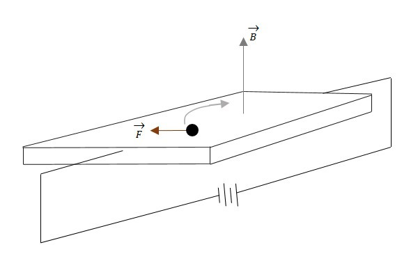
As electrons travel through the conductor that lies in a magnetic field B, the electrons will experience a magnetic force. This magnetic force will cause the electrons to travel close to one side than the other. This creates a negative charge on one side and positive charge on the other, as shown in the following figure.
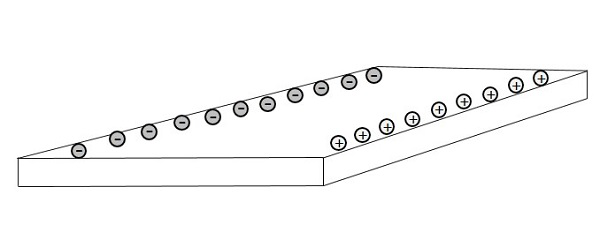
This separation of charge will create a voltage difference which is known as Hall Voltage or Hall EMF. The voltage builds up until the electric field produces an electric force on the charge that is equal and opposite of the magnetic force. This effect is known as Hall Effect.
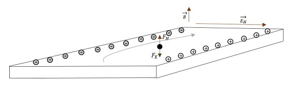
$$\overrightarrow{F_{magnetic}}\:\:=\:\:\overrightarrow{F_{Electric}}\:\:=\:\:q\:\:\overrightarrow{V_{D}}\:\:\overrightarrow{B}\:\:=\:\:q\:\:\overrightarrow{E_{H}}$$
VD is the velocity that every electron is experiencing
$\overrightarrow{E_{H}}\:\:=\:\:\overrightarrow{V_{D}}\:\:\overrightarrow{B}\:\:$ Since V = Ed
Where q = quantity of charge
$\overrightarrow{B}$ = the magnetic field
$\overrightarrow{V_{D}}$ = the drift velocity
$\overrightarrow{E_{H}}$ = the Hall electric effect
d = distance between the planes in a conductor (width of the conductor)
$$V_{H}\:\:=\:\:\varepsilon_{H}\:\:=\:\:\overrightarrow{E_{H}}\:\:d\:\:=\:\:\overrightarrow{V_{D}}\:\:\overrightarrow{B}\:\:d$$
$$\varepsilon_{H}\:\:=\:\:\overrightarrow{V_{D}}\:\:\overrightarrow{B}\:\:d$$
This is the Hall EMF
Uses
The Hall Effect is used for obtaining information regarding the semiconductor type, the sign of charge carriers, to measure electron or hole concentration and the mobility. There by, we can also know whether the material is a conductor, insulator or a semiconductor. It is also used to measure magnetic flux density and power in an electromagnetic wave.
Types of Currents
Coming to the types of currents in semiconductors, there are two terms need to be discussed. They are Diffusion Current and Drift Current.
Diffusion current
When doping is done, there occurs a difference in the concentration of electrons and holes. These electrons and holes tend to diffuse from higher concentration of charge density, to lower concentration level. As these are charge carriers, they constitute a current called diffusion current.
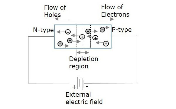
To know about this in detail, let us consider an N-type material and a P-type material.
N-type material has electrons as majority carriers and few holes as minority carriers.
P-type material has holes as majority carriers and few electrons as minority carriers.
If these two materials are brought too close to each other to join, then few electrons from valence band of N-type material, tend to move towards P-type material and few holes from valence band of P-type material, tend to move towards N-type material. The region between these two materials where this diffusion takes place, is called as Depletion region.
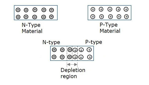
Hence, the current formed due to the diffusion of these electrons and holes, without the application of any kind of external energy, can be termed as Diffusion Current.
Drift Current
The current formed due to the drift (movement) of charged particles (electrons or holes) due to the applied electric field, is called as Drift Current. The following figure explains the drift current, whether how the applied electric field, makes the difference.
The amount of current flow depends upon the charge applied. The width of depletion region also gets affected, by this drift current. To make a component function in an active circuit, this drift current plays an important role.
Basic Electronics - Resistors
Resist is the word which means to oppose. Resistance is the property of opposing the flow of electrons, in a conductor or a semiconductor. A Resistor is an electronic component which has the property of resistance.
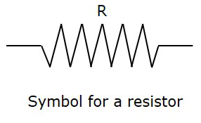
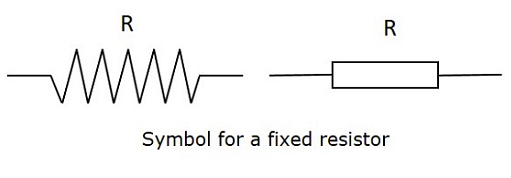
Symbol and Units
The symbol for a Resistor is as shown below.
The units of resistance is Ohms, which is indicated by Ω (omega).
The formula for resistance is
R = V/I
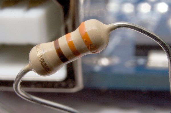
Where V is Voltage and I is Current. It would really be difficult to manufacture the resistors with each and every value. Hence, few values are chosen and the resistors of such values are only manufactured. These are called as Preferred Values. In practice, the resistors with near values are chosen to match the required applications. This is how a practical resistor looks like −
Color Coding
A process called color coding is used to determine the value of resistance for a resistor, just as shown in the above figure. A resistor is coated with four color bands where each color determines a particular value. The below table shows a list of values which each color indicates.
| COLOUR | DIGIT | MULTIPLIER | TOLERANCE |
|---|---|---|---|
| Black | 0 | 100 = 1 | |
| Brown | 1 | 101 = 10 | 1 |
| Red | 2 | 102 = 100 | 2 |
| Orange | 3 | 103 = 1000 | |
| Yellow | 4 | 104 = 10000 | |
| Green | 5 | 105 = 100000 | 0.5 |
| Blue | 6 | 106 = 1000000 | 0.25 |
| Violet | 7 | 107 = 10000000 | 0.1 |
| Gray | 8 | 108 = 100000000 | |
| White | 9 | 109 = 1000000000 | |
| Gold | 10-1 = 0.1 | 5 | |
| Silver | 10-2 = 0.01 | 10 | |
| (none) | 20 |
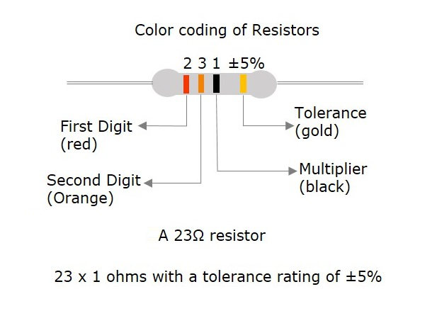
The first two colored bands indicate the first and second digit of the value and the third color band represents the multiplier (number of zeroes added). The fourth color band indicates the tolerance value.
Tolerance is the range of value up to which a resistor can withstand without getting destroyed. This is an important factor. The following figure shows how the value of a resistor is determined by color code.
The five color band resistors are manufactured with tolerance of 2% and 1% and also for other high accuracy resistors. In these five band resistors, the first three bands represent digits, fourth one indicates multiplier and the fifth represents tolerance.
Let us look at an example to understand the color coding process.
Example 1 − Determine the value of a resistor with a color code yellow, blue, orange and silver.
Solution − The value of yellow is 4, blue is 6, orange is 3 which represents multiplier. Silver is 10 which is the tolerance value.
Hence the value of the resistor is 46×103 = 46kΩ
The maximum resistance value for this resistor is
46kΩ or 46000Ω + 10% = 46000 + 4600 = 50600Ω = 50.6kΩ
The minimum resistance value for this resistor is
46kΩ or 46000Ω - 10% = 46000 - 4600 = 41400Ω = 41.4kΩ
After having gone through different details regarding resistors, we have some terms to learn. Also we have to deal with different behaviors of a resistor for few types of connections.
Important Terms
There are a few terms which we need to discuss before going into the type of resistors we have. One needs to get introduced to these terms at this stage and can understand them as we progress further.
Resistance
Resistance is the property of a resistor that opposes the flow of current. When alternating current goes through a resistance, a voltage drop is produced that is in-phase with the current.
Indication − R
Units − Ohms
Symbol − Ω
Along with resistance, there are other important terms, called as reactance and impedance.
Reactance
The resistance offered to the alternating current because of the capacitances and inductances present in the circuit, can be understood as reactance. When alternating current goes through a pure reactance, a voltage drop is produced that is 90out of phase with the current.
Depending upon the phase i.e., +90 or -90 the reactance can be termed as inductive reactance or capacitive reactance.
Indication − X
Units − Ohms
Symbol − Ω
Impedance
Impedance is the effective resistance to alternating current arising from the combined effects of ohmic resistance and reactance. When alternating current goes through an impedance, a voltage drop is produced which is somewhere between 0to 90out of phase with the current.
Indication − I
Units − Ohms
Symbol − Ω
Conductance
This is the ability of a material to conduct electricity. It is the reciprocal of resistance.
Indication − G
Units − Mhos
Symbol − ℧
Circuit Connections in Resistors
A Resistor when connected in a circuit, that connection can be either series or parallel. Let us now know what will happen to the total current, voltage and resistance values if they are connected in series as well, when connected in parallel.
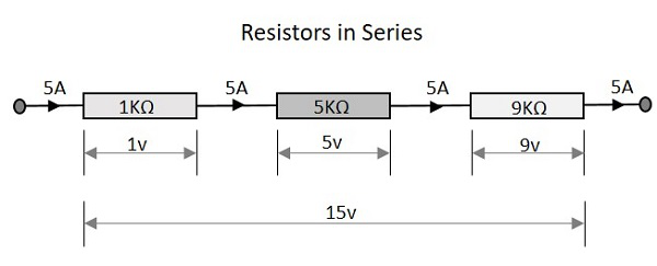
Resistors in Series
Let us observe what happens, when few resistors are connected in Series. Let us consider three resistors with different values, as shown in the figure below.
Resistance
The total resistance of a circuit having series resistors is equal to the sum of the individual resistances. That means, in the above figure there are three resistors having the values 1KΩ, 5KΩ and 9KΩ respectively.
Total resistance value of the resistor network is −
$$R\:\:=\:\:R_{1}\:+\:R_{2}\:+\:R_{3}$$
Which means 1 + 5 + 9 = 15KΩ is the total resistance.
Where R1 is the resistance of 1st resistor, R2 is the resistance of 2nd resistor and R3 is the resistance of 3rd resistor in the above resistor network.
Voltage
The total voltage that appears across a series resistors network is the addition of voltage drops at each individual resistances. In the above figure we have three different resistors which have three different values of voltage drops at each stage.
Total voltage that appears across the circuit −
$$V\:\:=\:\:V_{1}\:+\:V_{2}\:+\:V_{3}$$
Which means 1v + 5v + 9v = 15v is the total voltage.
Where V1 is the voltage drop of 1st resistor, V2 is the voltage drop of 2nd resistor and V3 is the voltage drop of 3rd resistor in the above resistor network.
Current
The total amount of Current that flows through a set of resistors connected in series is the same at all the points throughout the resistor network. Hence the current is same 5A when measured at the input or at any point between the resistors or even at the output.
Current through the network −
$$I\:\:=\:\:I_{1}\:=\:I_{2}\:=\:I_{3}$$
Which means that current at all points is 5A.
Where I1 is the current through the 1st resistor, I2 is the current through the 2nd resistor and I3 is the current through the 3rd resistor in the above resistor network.
Resistors in Parallel
Let us observe what happens, when few resistors are connected in Parallel. Let us consider three resistors with different values, as shown in the figure below.
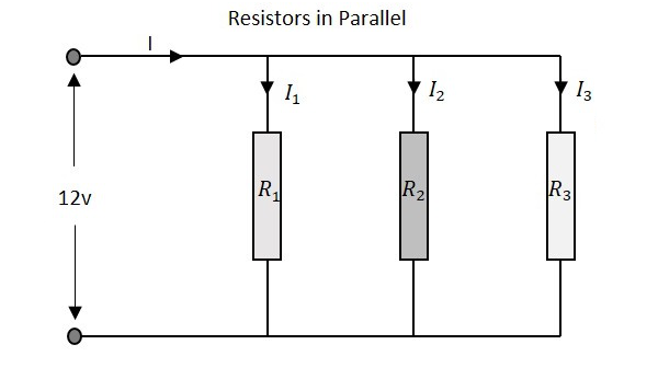
Resistance
The total resistance of a circuit having Parallel resistors is calculated differently from the series resistor network method. Here, the reciprocal (1/R) value of individual resistances are added with the inverse of algebraic sum to get the total resistance value.
Total resistance value of the resistor network is −
$$\frac{1}{R}\:\:=\:\:\frac{1}{R_{1}}\:\:+\:\:\frac{1}{R_{2}}\:\:+\frac{1}{R_{3}}$$
Where R1 is the resistance of 1st resistor, R2 is the resistance of 2nd resistor and R3 is the resistance of 3rd resistor in the above resistor network.
For example, if the resistance values of previous example are considered, which means R1 = 1KΩ, R2 = 5KΩ and R3 = 9KΩ. The total resistance of parallel resistor network will be −
$$\frac{1}{R}\:\:=\:\:\frac{1}{1}\:\:+\:\:\frac{1}{5}\:\:+\frac{1}{9}$$
$$=\:\:\frac{45\:\:+\:\:9\:\:+\:\:5}{45}\:\:=\:\:\frac{59}{45}$$
$$R\:\:=\:\:\frac{45}{59}\:\:=\:\:0.762K\Omega\:\:=\:\:76.2\Omega$$
From the method we have for calculating parallel resistance, we can derive a simple equation for two-resistor parallel network. It is −
$$R\:\:=\:\:\frac{R_{1}\:\:\times\:\:R_{2}}{R_{1}\:\:+\:\:R_{2}}\:$$
Voltage
The total voltage that appears across a Parallel resistors network is same as the voltage drops at each individual resistance.
The Voltage that appears across the circuit −
$$V\:\:=\:\:V_{1}\:=\:V_{2}\:=\:V_{3}$$
Where V1 is the voltage drop of 1st resistor, V2 is the voltage drop of 2nd resistor and V3 is the voltage drop of 3rd resistor in the above resistor network. Hence the voltage is same at all the points of a parallel resistor network.
Current
The total amount of current entering a Parallel resistive network is the sum of all individual currents flowing in all the Parallel branches. The resistance value of each branch determines the value of current that flows through it. The total current through the network is
$$I\:\:=\:\:I_{1}\:+\:I_{2}\:+\:I_{3}$$
Where I1 is the current through the 1st resistor, I2 is the current through the 2nd resistor and I3 is the current through the 3rd resistor in the above resistor network. Hence the sum of individual currents in different branches obtain the total current in a parallel resistive network.
A Resistor is particularly used as a load in the output of many circuits. If at all the resistive load is not used, a resistor is placed before a load. Resistor is usually a basic component in any circuit.
Basic Electronics - Non linear Resistors
There are many types of resistors according to the type of material used, the manufacturing procedure and their applications. The classification is as shown below.
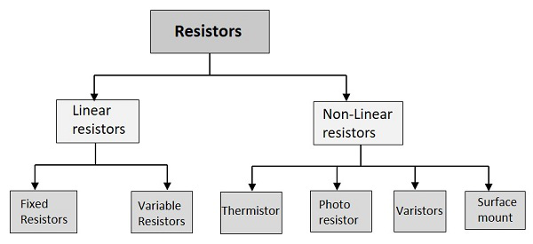
Linear resistors have linear VI characteristics and non-linear resistors has non-linear VI characteristics. Non-linear resistors are the resistors whose voltage and current characteristics vary non-linearly. The voltage and current values vary depending upon other factors like temperature and light, but they may not be linear.
Thermistor
Thermal means temperature. In this resistor, the resistance varies with temperature. If heat increases, the resistance decreases and vice versa. This is used for measurement and control purposes.
The main types of thermistors are NTC and PTC.
NTC is Negative Temperature Coefficient and in such devices, the resistance decreases as the temperature increases. These are used to protect the devices from over-voltage conditions.
PTC is Positive Temperature Coefficient and in such devices, the resistance increases as the temperature increases. These are used to protect the devices from over current conditions.
The following figure shows an NTC thermistor, along with its symbol.
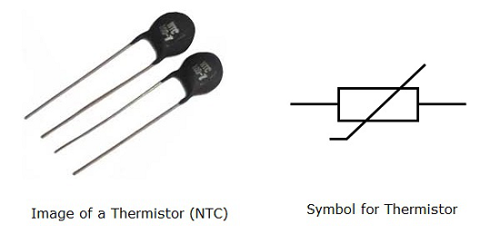
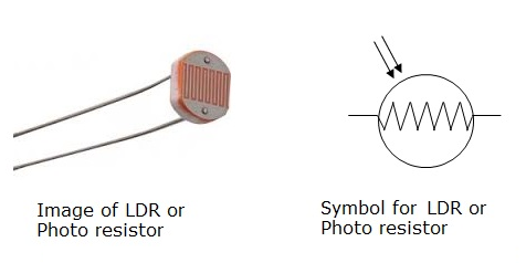
Photo Resistor
Photo means light. In this resistor, the resistance varies with light. As light increases resistance decreases and vice versa. This is also used for measurement and control purposes. It is also called as LDR (Light Dependent Resistor)
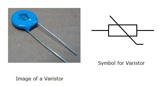
Varistors
The resistance of a varistor, varies with the applied voltage. As the voltage increases, the resistance decreases and if the voltage decreases, the resistance increases. It is also called as VDR (Voltage Dependent Resistor).
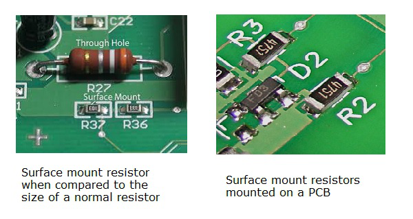
Surface Mount
These are being highly used since the introduction of surface mount technology. These can be termed as chip resistors, which means a resistive layer integrated on a ceramic chip.
These surface mount resistors are very small when compared to the normal resistors and hence occupy less space. They are effective and dissipate less heat. The invention of these resistors has changed the look of a PCB (Printed Circuit Board) and reduced its size greatly.
The advantages of surface mount resistors are −
- These are compact in size.
- These are very stable.
- They have good tolerance.
- They are effective in reducing heat dissipation.
The following figure shows the images of surface mount resistors.
Basic Electronics - Linear Resistors
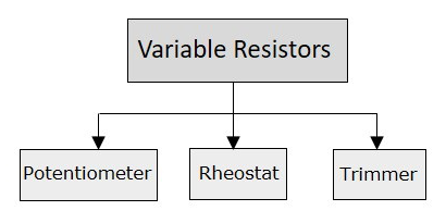
A Linear resistor is one whose resistance doesnt vary with the flow of current through it. The current through it, will always be proportional to the voltage applied across it. Linear resistors are further classified as Fixed and Variable resistors.
Variable Resistors
Variable resistors are those whose values can be varied manually, according to the requirement. A particular value of resistance is chosen from a range of resistance values, with the help of a shaft connected. The symbol of a variable resistor is as shown below.
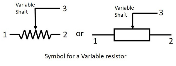
These resistors are better understood with the help of the classification we have. Variable resistors are further divided into Potentiometers, Rheostats and Trimmers.
Potentiometer
A Potentiometer is simply called as a Pot. This is a three-terminal resistor having a shaft which slides or rotates. This shaft when operated forms an adjustable voltage divider. The following figure shows an image of a Potentiometer.
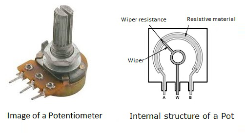
A potentiometer also measures the potential difference (voltage) in a circuit. A path of resistive material with resistance of low to high value is laid internally and a wiper is placed so that it connects the resistive material to the circuit. This is mostly used as a volume controller in TV sets and Music systems.
Rheostat
A Rheostat can be simply called as a Wire wound resistor. A Resistive wire is wound around an insulating ceramic core tightly. A Wiper slides over these windings. One connection is made to one end of the resistive wire and the second connection is made to the wiper or the sliding contact, to obtain the desired resistance.
The Rheostat is used to control current. These are mostly used in the speed control of heavy motors. The resistance obtained by these is in the order of kilo ohms. Rheostats are mostly available as single tube and double tube rheostats, as shown in the following figure.
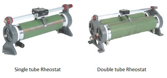
As a variable resistance they are often used for tuning and calibration in circuits. Now-a-days, the usage of rheostats was replaced by switching electronic devices, as rheostats have lower efficiency.
Trimmer
Trimmer is both a variable resistor and a potentiometer (measures potential difference). This Trimmer Potentiometer is, in short called as Trim Pot. If these are used as variable resistors, then they are called as Preset Resistors.
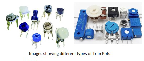
These trim pots are of different types such as single turn or multi turn. These are small variable resistors used for tuning and calibration. Their life span is shorter than other variable resistors.
Basic Electronics - Fixed Resistors
Fixed resistors are one type of linear resistors. A resistor is said to be a fixed resistor, if its value is fixed. The value of fixed resistor cant be varied like a variable resistor as its value is determined at the time of manufacturing itself. The following figures represent the symbol of a fixed resistor.
The fixed resistors are classified into different types, depending upon their manufacturing processes and the materials used in their manufacturing. The classification is as follows.
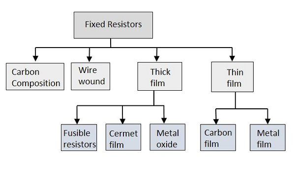
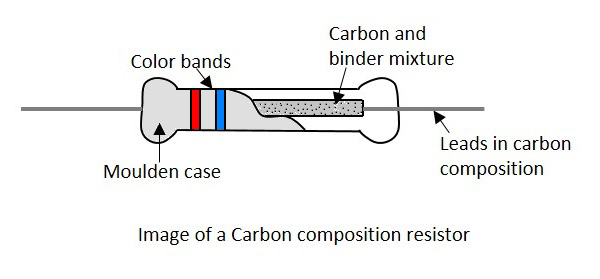
Carbon composition
The Carbon composition resistors are a blend of carbon particles, graphite and ceramic dust mixed with a binder substance like clay. This mixture is treated with high pressure and temperature. After the whole thing is molded in a case, the leads are fixed.
Thermal mass of the carbon composition resistor is higher so as to withstand high energy pulses.
These resistors have low stability and high noise which is a disadvantage.
The following figure shows an image of carbon composition resistor.
Carbon composition resistors are used in Surge protection, Current limiting, and High voltage power supplies.
Wire wound
A Wire wound resistor is formed by wounding a wire made up of a resistive material around a core. The metallic core acts as a non-conductive material while the resistive wire conducts, but with some resistance. The image of a wire wound resistor is as shown below.
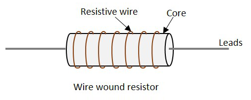
Usually a nichrome wire or a manganin wire is used to wind the core because they offer high resistance. Whereas plastic, ceramic or glass is used for core.
- Wire wound resistors are very accurate.
- They work excellently for low resistance values and high power ratings.
These are the oldest type of fixed resistors, but are being used even now.
Thick Film
The film resistors have a resistive layer on a ceramic base, whose thickness defines the type they belong to. The thickness of resistive layer on thick film resistors is much higher than thin film resistors. Thick film resistors are produced by firing a special paste, which is a mixture of glass and metal oxides, onto the substrate.
There are three main types in thick film resistors like Fusible resistors, Cermet film resistors, and Metal oxide film resistors.
Fusible Resistors
The Fusible resistors are similar to wire wound resistors. But these resistors along with providing resistance, act as a fuse. The image of a fusible resistor is as shown below.
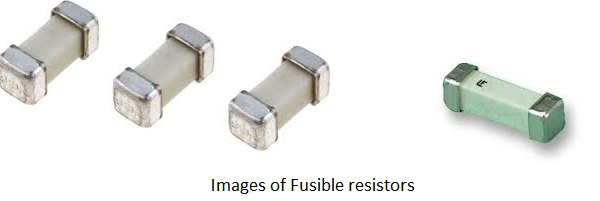
In this resistor, the current flows through a spring loaded connection, which is placed closely to the body of the resistor. The blob that is attached to the spring wire of the resistor takes the heat generated by the resistor due to the current flow. If this heat is increased, the attachment to the blob gets melted up and opens the connection.
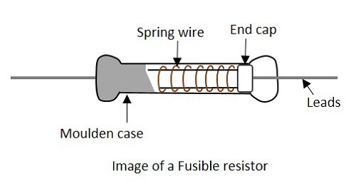
Hence we can say that, these resistors limit the current, but if the circuit power rating exceeds a specified value, these resistors act as a fuse to open or break the circuit. The value of these resistors is usually of less than 10 Ohms. These resistors are generally used in TV sets, amplifiers and other expensive electronic circuits.
Cermet Film Resistors
The Cermet film resistors are the film resistors made up of a special material called Cermet. Cermet is a composite alloy made by combining Ceramic and Metal. This combination provides the advantages in both of these materials like high temperature resistance and wear resistance of ceramic along with flexibility and electrical conductivity of a metal.
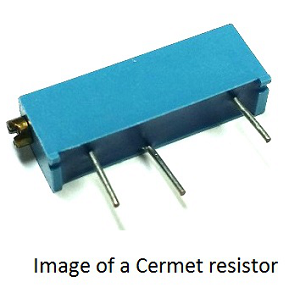
A metal film layer is wrapped around a resistive material and is fixed in a ceramic metal or cermet substrate. Leads are taken to make the connections easy while fixing on a PCB. They offer high stability as temperature cannot affect their performance.
Metal Oxide film resistors
A Metal oxide film resistor is formed by oxidizing a thick film of Tin chloride on a heated glass rod, which is a substrate. They have high temperature stability and can be used at high voltages. These resistors have low operating noise.
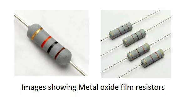
Metal oxide film resistors differ with metal film ones only regarding the type of film coated. Metal oxide is a metallic compound like tin with oxygen to form tin oxide, which is coated as a film on the resistor. The resistivity of this resistor depends upon the amount of antimony oxide added to the tin oxide.
Thin Film
Thin film resistors have a resistive layer of width 0.1 micrometer or smaller on the ceramic base. Thin film resistors have a metallic film that is vacuum deposited on an insulating substrate.
Thin film resistors are more accurate and have better temperature coefficient and is more stable. The thin film resistors are further divided into two types such as −
- Carbon film resistors
- Metal film resistors
Carbon film resistor
A Carbon film resistor is made by depositing a carbon film layer on a ceramic substrate. The carbon film acts as the resistive material to the current and the ceramic substance acts as an insulating substance. Metallic caps are fixed at both the ends and copper leads are drawn out.
The following figure shows the construction of a carbon film resistor.
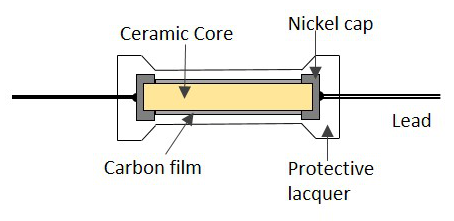
The main advantages of these resistors are their high stability, wide operating range, low noise, and low cost. The carbon film resistors are the most preferred ones over carbon composition resistors due to their low noise.
Metal Film Resistors
The film coating makes the difference between metal oxide film resistors and metal film resistors. A thin film of metallic substance such as nickel chromium is used to coat the resistor in a metal film resistor whereas a film of metal oxide like tin oxide is used to coat the resistor in a metal oxide resistor.
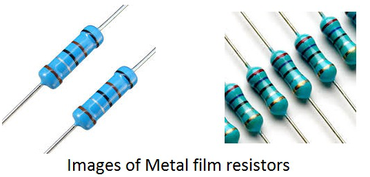
Metal film resistors have low temperature coefficient of resistance, which means the resistance is less affected by the temperature.
Wattage
While using a resistor, if the flow of current increases, the resistor dissipates some heat. If this value crosses a certain critical value, the resistor may get damaged. The wattage rating of a resistor is printed on some higher value resistors in order to avoid such situation.
Wattage is the amount of electric power expressed in watts. Electric power is the rate of transfer of electrical energy.
Power P = VI = I2R
Basic Electronics - Capacitors
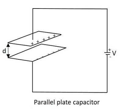
A Capacitor is a passive component that has the ability to store the energy in the form of potential difference between its plates. It resists a sudden change in voltage. The charge is stored in the form of potential difference between two plates, which form to be positive and negative depending upon the direction of charge storage.
A non-conducting region is present between these two plates which is called as dielectric. This dielectric can be vacuum, air, mica, paper, ceramic, aluminum etc. The name of the capacitor is given by the dielectric used.
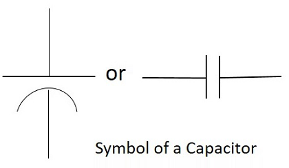
Symbol and Units
The standard units for capacitance is Farads. Generally, the values of capacitors available will be in the order of micro-farads, pico-farads and nano-farads. The symbol of a capacitor is as shown below.
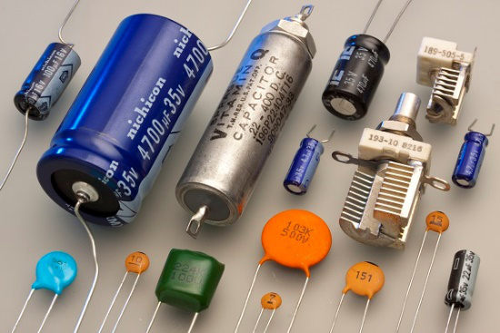
The Capacitance of a capacitor is proportional to the distance between the plates and is inversely proportional to the area of the plates. Also, the higher the permittivity of a material, the higher will be the capacitance. The permittivity of a medium describes how much electric flux is being generated per unit charge in that medium. The following image shows some practical capacitors.
When two plates having same area A, and equal width are placed parallel to each other with a separation of distance d, and if some energy is applied to the plates, then the capacitance of that parallel plate capacitor can be termed as −
$$C\:\:=\:\:\frac{\varepsilon_{0}\:\:\varepsilon_{r}\:\:d}{A}$$
Where
C = Capacitance of a capacitor
$\varepsilon_{0}$ = permittivity of free space
$\varepsilon_{r}$ = permittivity of dielectric medium
d = distance between the plates
A = area of the two conducting plates
With some voltage applied, the charge deposits on the two parallel plates of the capacitor. This charge deposition occurs slowly and when the voltage across the capacitor equals the voltage applied, the charging stops, as the voltage entering equals the voltage leaving.
The rate of charging depends upon the value of capacitance. The greater the value of capacitance, the slower the rate of change of voltage in the plates.
Working of a Capacitor
A Capacitor can be understood as a two-terminal passive component which stores electrical energy. This electrical energy is stored in electrostatic field.
Initially, the negative and positive charges on two plates of the capacitor are in equilibrium. There is no tendency for a capacitor to get charged or discharged. The negative charge is formed by the accumulation of electrons, while the positive charge is formed by the depletion of electrons. As this happens without any external charge given, this state is electrostatic condition. The figure below shows the capacitor with static charges.
The accumulation and depletion of electrons according to the varying positive and negative cycles of the AC supply, can be understood as current flow. This is called as Displacement Current. The direction of this current flow keeps on changing as this is AC.
Charging of a Capacitor
When an external voltage is given, the electric charge gets converted into electrostatic charge. This happens while the capacitor is charging. The positive potential of the supply, attracts the electrons from the positive plate of the capacitor, making it more positive. While the negative potential of the supply, forces the electrons to the negative plate of the capacitor, making it more negative. The figure below explains this.
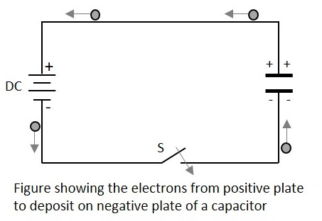
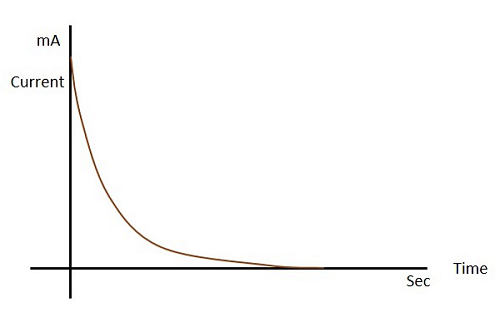
During this process of charging, the electrons move through the DC supply but not through the dielectric which is an insulator. This displacement is large, when the capacitor starts to charge but reduces as it charges. The capacitor stops charging when the voltage across capacitor equals the supply voltage.
Let us see what happens to the dielectric when the capacitor begins to charge.
Dielectric behavior
As the charges deposit on the plates of the capacitor, an electrostatic field is formed. The strength of this electrostatic field depends upon the magnitude of charge on the plate and the permittivity of the dielectric material. Permittivity is the measure of dielectric whether how far it allows the electrostatic lines to pass through it.
The dielectric is actually an insulator. It has electrons in the outer most orbit of the atoms. Let us observe how they get affected. When there is no charge on the plates, the electrons in the dielectric move in circular orbit. This is as shown in the figure below.
When charge deposition takes place, the electrons tend to move towards the positive charged plate, but still they keep on revolving as shown in the figure.
If the charge increases further, the orbits expand more. But if it still increases, the dielectric breaks down shorting the capacitor. Now, the capacitor being fully charged, its ready to get discharged. It is enough if we provide a path for them to travel from negative to positive plate. The electrons flow without any external supply as there are too many number of electrons on one side and barely any electrons on the other. This imbalance is adjusted by the discharge of the capacitor.
Also, when a discharge path is found, the atoms in the dielectric material tend to get to their normal circular orbit and hence forces the electrons to get discharged. This kind of discharge enables capacitors to deliver high currents in a short period of time, just as in a camera flash.
Color Coding
To know the value of a capacitor, it is usually labelled as below −
n35 = 0.35nF or 3n5 = 3.5nF or 35n = 35nF and so on.
Sometimes the markings will be like 100K which means, k = 1000pF. Then the value will be 100 × 1000pF = 100nF.
Though these number markings are being used now-a-days, an International color coding scheme was developed long ago, to understand the values of capacitors. The color coding indications are just as given below.
| Band colour | Digit A and B | Multiplier | Tolerance (t) > 10pf | Tolerance (t) < 10pf | Temperature coefficient |
|---|---|---|---|---|---|
| Black | 0 | × 1 | ±20% | ±2.0pF | |
| Brown | 1 | × 10 | ±1% | ±0.1pF | -33 × 10-6 |
| Red | 2 | × 100 | ±2% | ±0.25pF | -75 × 10-6 |
| Orange | 3 | × 1,000 | ±3% | -150 × 10-6 | |
| Yellow | 4 | × 10,000 | ±4% | -220 × 10-6 | |
| Green | 5 | × 100,000 | ±5% | ±0.5pF | -330 × 10-6 |
| Blue | 6 | × 1,000000 | -470 × 10-6 | ||
| Violet | 7 | -750 × 10-6 | |||
| Gray | 8 | × 0.01 | +80%, -20% | ||
| White | 9 | × 0.1 | ±10% | ±1.0pF | |
| Gold | × 0.1 | ±5% | |||
| Silver | × 0.01 | ±10% |
These indications were used to identify the value of capacitors.
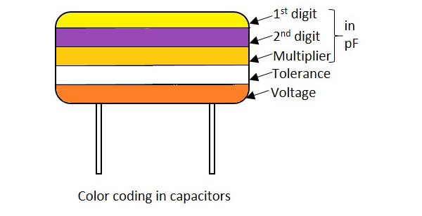
In these five band capacitors, the first two bands represent digits, third one indicates multiplier, fourth for tolerance and the fifth represents voltage. Let us look at an example to understand the color coding process.
Example 1 − Determine the value of a capacitor with a color code yellow, violet, orange, white and red.
Solution − The value of yellow is 4, violet is 7, orange is 3 which represents multiplier. White is ±10 which is the tolerance value. Red represents the voltage. But to know the voltage rating, we have got another table, from which the particular band to which this capacitor belongs, has to be known.
Hence the value of the capacitor is 47nF, 10% 250v (voltage for V band)
The following table shows how voltage is determined depending upon the bands the capacitors belong to.
| Band colour | Voltage Rating (V) | ||||
|---|---|---|---|---|---|
| TYPE J | TYPE K | TYPE L | TYPE M | TYPE N | |
| Black | 4 | 100 | 10 | 10 | |
| Brown | 6 | 200 | 100 | 1.6 | |
| Red | 10 | 300 | 250 | 4 | 35 |
| Orange | 15 | 400 | 40 | ||
| Yellow | 20 | 500 | 400 | 6.3 | 6 |
| Green | 25 | 600 | 16 | 15 | |
| Blue | 35 | 700 | 630 | 20 | |
| Violet | 50 | 800 | |||
| Gray | 900 | 25 | 25 | ||
| White | 3 | 1000 | 2.5 | 3 | |
| Gold | 2000 | ||||
| Silver | |||||
With the help of this table, the voltage rating for each band of capacitors is known according to the color given. The type of voltage ratings also indicates the type of capacitors. For example, TYPE J ones are Dipped Tantalum Capacitors, TYPE K ones are Mica Capacitors, TYPE L ones are Polystyrene Capacitors, TYPE M ones are Electrolytic Band 4 Capacitors and TYPE N ones are Electrolytic Band 3 Capacitors. These days, the color coding has been replaced by simple printing of value of the capacitors as mentioned previously.
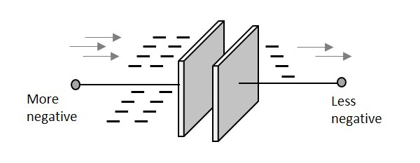
Capacitive Reactance
This is an important term. Capacitive Reactance is the opposition offered by a capacitor to the alternating current flow, or simply AC current. A capacitor resists the change in the flow of current and hence it shows some opposition which can be termed as reactance, as the frequency of the input current should also be considered along with the resistance it offers.
Symbol: XC
In a purely capacitive circuit, the current IC leads the applied voltage by 90
Temperature Coefficient of Capacitors
The maximum change in Capacitance of a capacitor, over a specified temperature range, can be known by the temperature coefficient of a capacitor. It states that when the temperature exceeds a certain point, the change in capacitance of a capacitor that might occur is understood as the temperature coefficient of capacitors.
All the capacitors are usually manufactured considering a reference temperature of 25C. Hence the temperature coefficient of capacitors is considered for the values of temperatures that are above and below this value.
Circuit Connections in Capacitors
In a circuit, a Capacitor can be connected in series or in parallel fashion. If a set of capacitors were connected in a circuit, the type of capacitor connection deals with the voltage and current values in that network.
Capacitors in Series
Let us observe what happens, when few Capacitors are connected in Series. Let us consider three capacitors with different values, as shown in the figure below.
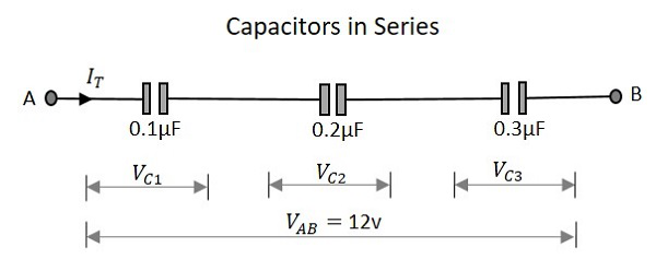
Capacitance
When the capacitance of a network whose capacitors are in series is considered, the reciprocal of the capacitances of all capacitors, is added to get the reciprocal of the total capacitance. To get this more clearly,
$$\frac{1}{C_{T}}\:\:=\:\:\frac{1}{C_{1}}\:\:+\:\:\frac{1}{C_{2}}\:\:+\:\:\frac{1}{C_{3}}$$
Following the same formula, if simply two capacitors are connected in series, then
$$C_{T}\:\:=\:\:\frac{C_{1}\:\:\times\:\:C_{2}}{C_{1}\:\:+\:\:C_{2}}$$
Where C1 is the capacitance across the 1st capacitor, C2 is the capacitance across the 2nd capacitor and C3 is the capacitance across the 3rd capacitor in the above network.
Voltage
The voltage across each capacitor depends upon the value of individual capacitances. Which means
$$V_{C1}\:\:=\:\:\frac{Q_{T}}{C_{1}}\:\:V_{C2}\:\:=\:\:\frac{Q_{T}}{C_{2}}\:\:V_{C3}\:\:=\:\:\frac{Q_{T}}{C_{3}}$$
The total voltage across the series capacitors circuit,
$$V_{T}\:\:=\:\:V_{C1}\:\:+\:\:V_{C2}\:\:+\:\:V_{C3}$$
Where Vc1 is the voltage across the 1st capacitor, Vc2 is the voltage across the 2nd capacitor and Vc3 is the voltage across the 3rd capacitor in the above network.
Current
The total amount of Current that flows through a set of Capacitors connected in series is the same at all the points. Therefore the capacitors will store the same amount of charge regardless of their capacitance value.
Current through the network,
$$I\:\:=\:\:I_{1}\:\:=\:\:I_{2}\:\:=\:\:I_{3}$$
Where I1 is the current through the 1st capacitor, I2 is the current through the 2nd capacitor and I3 is the current through the 3rd capacitor in the above network.
As the current is same, the storage of charge is same because any plate of a capacitor gets its charge from the adjacent capacitor and hence capacitors in series will have the same charge.
$$Q_{T}\:\:=\:\:Q_{1}\:\:=\:\:Q_{2}\:\:=\:\:Q_{3}$$
Capacitors in Parallel
Let us observe what happens, when few capacitors are connected in Parallel. Let us consider three capacitors with different values, as shown in the figure below.
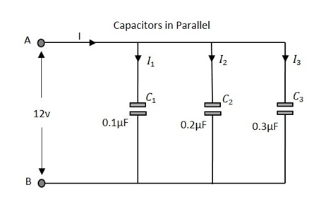
Capacitance
The total Capacitance of the circuit is the equivalent to the sum of the individual capacitances of the capacitors in the network.
$$C_{T}\:\:=\:\:C_{1}\:\:+\:\:C_{2}\:\:+\:\:C_{3}$$
Where C1 is the capacitance across the 1st capacitor, C2 is the capacitance across the 2nd capacitor and C3 is the capacitance across the 3rd capacitor in the above network.
Voltage
The voltage measured at the end of the circuit is same as the voltage across all the capacitors that are connected in a parallel circuit.
$$V_{T}\:\:=\:\:V_{1}\:\:=\:\:V_{2}\:\:=\:\:V_{3}$$
Where Vc1 is the voltage across the 1st capacitor, Vc2 is the voltage across the 2nd capacitor and Vc3 is the voltage across the 3rd capacitor in the above network.
Current
The total current flowing is equal to the sum of the currents flowing through each capacitor connected in the parallel network.
$$I_{T}\:\:=\:\:I_{1}\:\:+\:\:I_{2}\:\:+\:\:I_{3}$$
Where I1 is the current through the 1st capacitor, I2 is the current through the 2nd capacitor and I3 is the current through the 3rd capacitor in the above network.
Basic Electronics - Variable Capacitors
There are many types of capacitors depending upon their function, the dielectric material used, their shape etc. The main classification is done according to fixed and variable capacitors.
Types of Capacitors
The classification is as shown in the following figure.
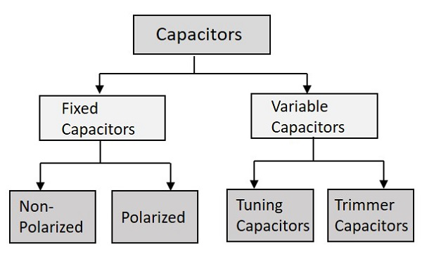
The main classification is just like the above one. The fixed capacitors are the ones whose value is fixed at the time of manufacturing itself and the variable ones provide us with an option to vary the value of capacitance.
Variable Capacitors
Let us know something about the variable capacitors whose value alters when you vary, either electrically or mechanically. Variable capacitors in general consists of interwoven sets of metallic plates in which one is fixed and the other is variable. These capacitors provide the capacitance values so as to vary between 10 to 500pF.
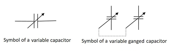
The ganged capacitor shown here is a combination of two capacitors connected together. A single shaft is used to rotate the variable ends of these capacitors which are combined as one. The dotted line indicates that they are connected internally.
There are many uses of these variable resistors such as for tuning in LC circuits of radio receivers, for impedance matching in antennas etc. The main types of variable capacitors are Tuning capacitors and Trimmer capacitors.
Tuning Capacitors
Tuning capacitors are popular type of variable capacitors. They contain a stator, a rotor, a frame to support the stator and a mica capacitor. The constructional details of a tuning capacitor are shown in the following figure.
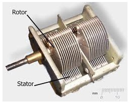
The stator is a stationary part and rotor rotates by the movement of a movable shaft. The rotor plates when moved into the slots of stator, they come close to form plates of a capacitor. When the rotor plates sit completely in the slots of the stator then the capacitance value is maximum and when they dont, the capacitance value is minimum.
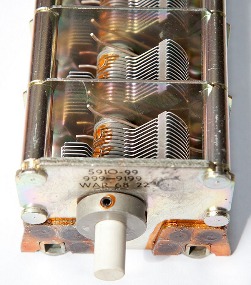
The above figure shows a ganged tuning capacitor having two tuning capacitors connected in a gang. This is how a tuning capacitor works. These capacitors generally have capacitance values from few Pico Farads to few tens of Pico Farads. These are mostly used in LC circuits in radio receivers. These are also called as Tuning Condensers.
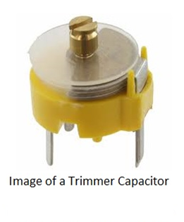
Trimmer Capacitors
Trimmer capacitors are varied using a screwdriver. Trimmer capacitors are usually fixed in such a place where there is no need to change the value of capacitance, once fixed.
There are three leads of a trimmer capacitor, one connected to stationary plate, one to rotary and the other one is common. The movable disc is a semi-circular shaped one. A trimmer capacitor would look like the ones in the following figure.
There are two parallel conducting plates present with a dielectric in the middle. Depending upon this dielectric used, there are air trimmer capacitors and ceramic trimmer capacitors. The constructional details of a trimmer capacitor are as shown below.
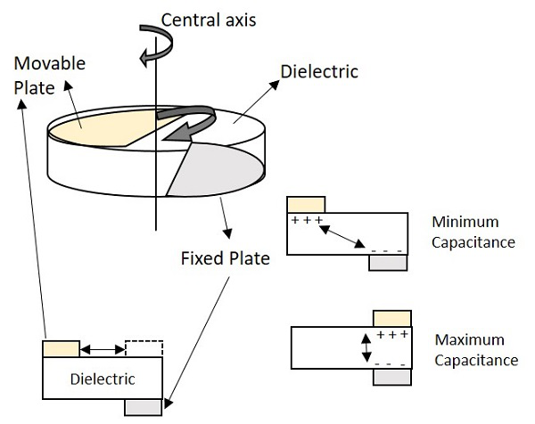
One of the two plates is movable, while the other is fixed. The dielectric material is fixed. When the movable plate is moved, opposite to the area between movable and fixed electrode, then the capacitance can be changed. The capacitance will be higher if the opposite area gets bigger, as both the electrodes act as two plates of a capacitor.
The Trimmer Capacitors are easily fixed on a PCB (Printed Circuit Board) and they are mostly used for calibration of equipment.
Basic Electronics - Fixed Capacitors
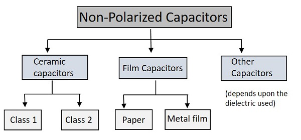
The Capacitors whose value is fixed while manufacturing and cannot be altered later are called as Fixed Capacitors. The main classification of fixed capacitors is done as polarized and non-polarized. Let us have a look at Non-polarized capacitors.
Non-Polarized Capacitors
These are the capacitors that have no specific polarities, which means that they can be connected in a circuit, either way without bothering about the placement of right lead and left lead. These capacitors are also called as Non-Electrolytic Capacitors.
The main classification of Non-Polarized capacitors is done as shown in the following figure.
Among the types of capacitors, let us first go through the Ceramic Capacitors.
Ceramic Capacitors
The common capacitors used among fixed type are Ceramic Capacitors. The Ceramic capacitors are fixed capacitors that have ceramic material as a dielectric.
These ceramic capacitors are further classified as class1 and class2 depending upon their applications. For instance, Class1 has high stability and works best for resonant circuit applications, while class2 has high efficiency and gives its best for coupling applications.
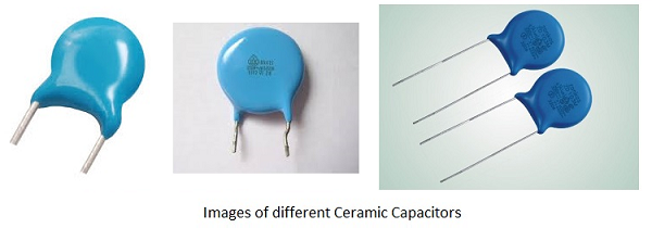
A hollow tubular or plate like ceramic material such as titanium dioxide and barium titanate is coated with a deposition of silver compound on both walls, so that both sides act as two capacitor plates and ceramic acts as a dielectric. Leads are drawn from these two surfaces and this whole assembly is encapsulated in a moisture-proof coating.
The most often used modern ceramic capacitors are Multi-Layer Chip Capacitors (MLCC). These capacitors are made in surface mounted technology and are mostly used due to their small size. These are available in the order of 1F to 100F.
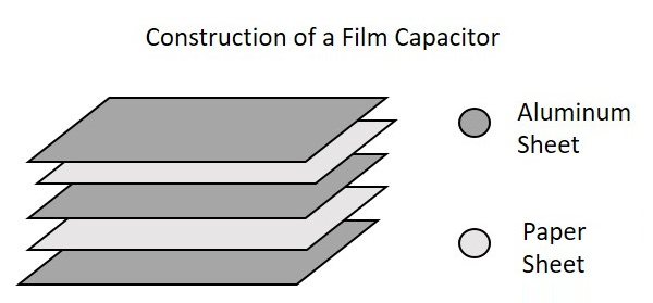
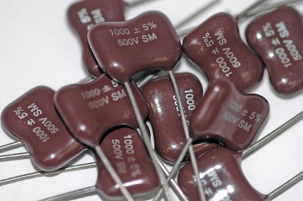
Film Capacitors
The Film Capacitors are the ones which have a film substance as a dielectric material. Depending upon the type of film used, these are classified as Paper and Metal film capacitors.
These film capacitors are both paper dielectric capacitors whereas a paper capacitor uses a waxed paper while a metallic film capacitor uses a metallized paper. The arrangement is almost same as shown below.
Paper Capacitors
Paper capacitors use Paper as a dielectric material. Two thin tin foil sheets are taken and placed between thin waxed or oiled paper sheets. This paper acts as a dielectric. Now-a-days paper is being replaced by plastic.
These sheets are sandwiched and are rolled into a cylindrical shape and encapsulated in a plastic enclosure. Leads are drawn out. The following figure shows an example of Paper Capacitors.
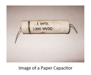
Paper capacitors are available in the order of 0.001F to 2F and the voltage rating can be as high as 2000volts. These capacitors are useful in high voltage and current applications.
Metal Film Capacitors
Metal Film capacitors are another type of film capacitors. These are also called as Metal Foil Capacitors or Metallized Paper Capacitors as the dielectric used here is a paper coated with metallic film.
Unlike in paper capacitors, a film of Aluminum or Zinc is coated on a paper to form a dielectric in this metallic film capacitors. Instead of Aluminum sheets placing between papers, the paper itself is directly coated here. This reduces the size of the capacitor.
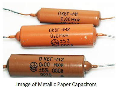
The Aluminum coating is preferred over zinc coating so as to avoid destruction of capacitor due to chemical reduction. The Aluminum coated sheets are rolled in the form of a cylinder and leads are taken. This whole thing is encapsulated with wax or plastic resin to protect the capacitor. These capacitors are useful in high voltage and current applications.
Other Capacitors
These are the miscellaneous capacitors that are named after the dielectric materials used. This group includes Mica Capacitors, Air Capacitors, Vacuum Capacitors and Glass Capacitors etc.
Mica Capacitors
The Mica Capacitors are made by using thin Mica sheets as dielectric materials. Just like paper capacitors, thin metal sheets are sandwiched with mica sheets in between. Finally the layers of metal sheets are connected at both ends and two leads are formed. Then the whole assembly is enclosed in plastic Bakelite capsule. The following image shows how a Mica capacitor looks like.
Mica Capacitors are available in the range of 50pF to 500pF. The Mica capacitors have high working voltage up to 500volts. These are most commonly used capacitors for electronic circuits such as ripple filters, Resonant circuits, Coupling circuits and high power, high current RF broadcast transmitters.
Air Capacitors
The Air Capacitors are the ones with air as dielectric. The simplest air capacitors are the ones with conducting plates having air in between. This construction is exactly the same as the variable tuning capacitor discussed above. These capacitors can be fixed and variable also but fixed are very rarely used as there are others with superior characteristics.
Vacuum Capacitors
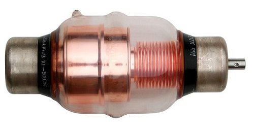
The Vacuum Capacitors uses high vacuum as dielectric instead of air or some other material. These are also available in fixed and variable modes. The construction of these capacitors is similar to vacuum tubes. They are mostly seen in the form of a glass cylinder which contain inter-meshed concentric cylinders.
The following image shows a variable vacuum capacitor.
The following image shows how a fixed vacuum capacitor looks like −
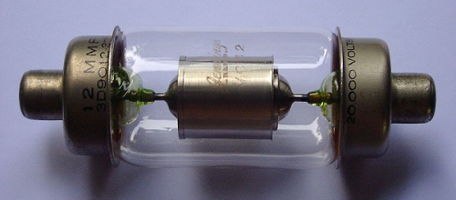
Variable vacuum capacitors are available at a range of 12pF to 5000pF and they are used for high voltage applications such as 5kV to 60kV. They are used in main equipment such as high power broadcast transmitters, RF amplifiers and large antenna tuners.
Glass Capacitors
Glass capacitors are very exclusive ones with many advantages and applications. As all of the above types, here glass is the dielectric substance. Along with glass dielectric, Aluminum electrodes are also present in these capacitors. Plastic encapsulation is done after taking out the leads. The leads can be axial leads or tubular leads.
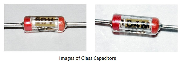
There are many advantages of a glass capacitor such as −
- The temperature coefficient is low.
- These are Noise-free capacitors.
- They produce high quality output with low loss.
- They have the capability of handling high operating temperatures.
- These capacitors can handle large RF currents.
There are many applications for these glass capacitors such as −
- Used in circuits that need to be at high temperature zones.
- Used in circuits that need high Q.
- Used in high power handling circuits.
- Used for circuits that need high tolerances.
Basic Electronics - Polarized Capacitors
Polarized Capacitors are the ones that have specific positive and negative polarities. While using these capacitors in circuits, it should always be taken care that they are connected in perfect polarities. The following image shows the classification of polarized capacitors.
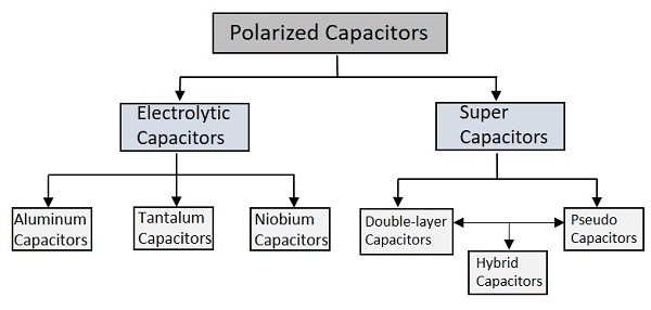
Lets start the discussion with Electrolytic Capacitors.
Electrolytic Capacitors
The Electrolytic Capacitors are the capacitors which indicate by the name that some electrolyte is used in it. They are polarized capacitors which have anode (+) and cathode (-) with particular polarities.
A metal on which insulating oxide layer forms by anodizing is called as an Anode. A solid or non-solid electrolyte which covers the surface of the oxide layer, functions as a cathode. The Electrolytic Capacitors have much higher Capacitance-Voltage (CV) value than the others, due to their larger anode surface and thin dielectric oxide layer.
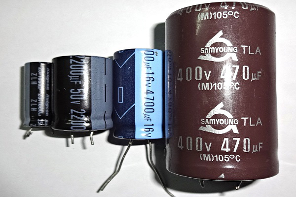
Aluminum Electrolytic Capacitors
Aluminum Electrolytic Capacitors are the most common types among the Electrolytic capacitors. In these ones, a pure Aluminum foil with an etched surface acts as an Anode. A thin layer of metal, which has a thickness of few micrometers acts as a diffusion barrier, which is placed between two metals to separate electrically. Hence the diffusion barrier acts as a dielectric. The electrolyte acts as a cathode which covers the rough surface of oxide layer.
The following figure shows an image of different sizes of Aluminum Electrolytic Capacitors available.
Depending upon the electrolyte there are three types of Aluminum Electrolytic Capacitors. They are −
- Wet Aluminum Electrolytic capacitors (non-solid)
- Manganese dioxide Aluminum Electrolytic capacitors (solid)
- Polymer Aluminum Electrolytic capacitors (solid)
The main advantage with these Aluminum Electrolytic capacitors is that, they have low impedance values even at mains frequency and they are cheaper. These are mostly used in Power supply circuits, SMPS (Switched Mode Power Supply) and DC-DC Converters.
Tantalum Electrolytic capacitors
These are another type of Electrolytic capacitors whose anode is made up of tantalum on which a very thin insulating oxide layer is formed. This layer acts as a dielectric and the electrolyte acts as a cathode which covers the surface of oxide layer.
The following figure shows how tantalum capacitors look like.
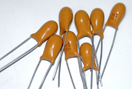
Tantalum provides high permittivity dielectric layer. Tantalum has high capacitance per volume and lower weight. But these ones are costlier than Aluminum Electrolytic capacitors, due to the frequent unavailability of tantalum.
Niobium Electrolytic Capacitors
A Niobium Electrolytic Capacitor is the other type of Electrolytic Capacitors in which a passivated niobium metal or niobium monoxide is considered as anode and an insulating niobium pentoxide layer is added on to the anode, so that it acts as a dielectric. A solid electrolyte is laid on the surface of the oxide layer which acts as a cathode. The following figure shows how Niobium capacitors look like.
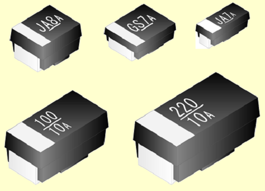
The Niobium Capacitors are commonly available as SMD (Surface Mount Devices) chip capacitors. These are easily fitted in a PCB. These capacitors should be operated in perfect polarities. Any kind of reverse voltage or ripple current higher than the specified will eventually destroy the dielectric and the capacitor as well.
Super Capacitors
The high capacity electrochemical capacitors with capacitance values much higher than the other capacitors, are called as Super Capacitors. These can be categorized as a group that lies between electrolytic capacitors and rechargeable batteries. These are also called as Ultra Capacitors.
There are many advantages with these capacitors such as −
- They have high capacitance value.
- They can store and deliver charge much faster.
- They can handle more charge and discharge cycles.
These capacitors have many applications such as −
- They are used in cars, buses, trains, elevators and cranes.
- They are used in regenerative braking.
- They are used for memory backup.
The types of super capacitors are Double-layered, Pseudo and Hybrid ones.
Double-layered Capacitors
Double-layered capacitors are electrostatic capacitors. The charge deposition is done in these capacitors according to the principle of Double-layer.
All solid substances have negative charge on the surface layer when disposed into a liquid.
This is due to the high dielectric coefficient of liquid.
All the positive ions come near the surface of the solid material to make a skin.
The deposition of positive ions near the solid material get looser with the distance.
The charge created at this surface due to the deposition of anions and cations leads to some capacitance value.
This double-layer phenomenon is also termed as Helmholtz double layer. The figure below explains the procedure of double-layer phenomenon, when the capacitor is charged and when it is discharged.
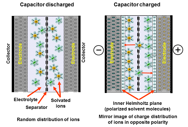
These capacitors are simply called as Electric Double Layered Capacitors (EDLC). They use carbon electrodes to achieve separation of charge between the surface of conductive electrode and the electrolyte. The carbon acts as dielectric and the other two as anode and cathode. The separation of charge is much smaller than in a conventional capacitor.
Pseudo Capacitors
These capacitors follow the electrochemical process for the deposition of charge. This is also called as faradaic process. At an electrode, when some chemical substance reduces or oxidizes, some current is generated. During such process, these capacitors store the electric charge by electron transfer between electrode and electrolyte. This is the working principle of Pseudo capacitors.
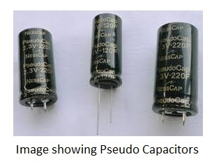
They get charged much faster and store the charge as much as a battery does. They are operated at a faster rate. These are used in tandem with batteries to improve life. These are used in grid applications to handle power fluctuations.
Hybrid Capacitors
A Hybrid Capacitor is a combination of EDLC and Pseudo Capacitor. In the Hybrid capacitors, activated carbon is used as cathode and the pre-doped carbon material acts as anode. Li ion capacitor is the common example of this type. The following figure shows different types of Hybrid Capacitors.
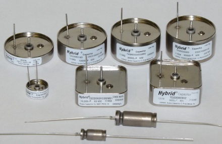
They have high tolerance in a wide range of temperature variations from -55C to 200C. Hybrid capacitors are also used in airborne applications. Though cost is high, these capacitors are highly reliable and compact. These are rugged and can tolerate extreme shock, vibration and pressure from environment. Hybrid capacitors have higher energy density and higher specific power than any electrolytic capacitor.
Basic Electronics - Inductors
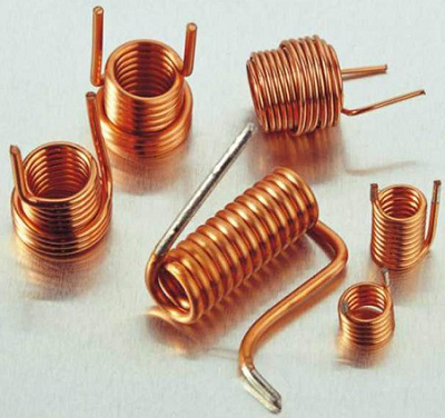
Let me introduce you to another important component in the field of Electronics and Electricals, the Inductor. Inductor is a passive two-terminal component that temporarily stores energy in the form of a magnetic field. It is usually called as a coil. The main property of an inductor is that it opposes any change in current.
Inductor
According to the Faradays law of Electromagnetic induction, When the current flowing through an inductor changes, the time-varying magnetic field induces a voltage in the conductor. According to lens law, the direction of induced EMF opposes the change in current that created it. Hence, induced EMF is opposite to the voltage applied across the coil. This is the property of an inductor.
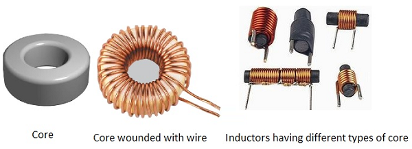
The following figure shows how an inductor looks like.
An inductor blocks any AC component present in a DC signal. The inductor is sometimes wrapped upon a core, for example a ferrite core. It then looks as in the figure below.
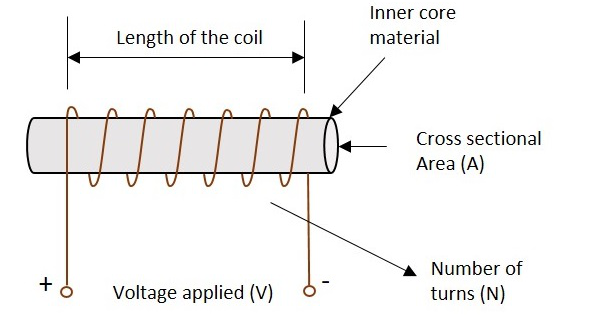
The following figure shows an inductor with various parts labelled.
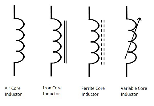
Symbols
The symbols of various types of inductors are as given below.
Storage of Energy
One of the Basic properties of electromagnetism is that the current when flows through an inductor, a magnetic field gets created perpendicular to the current flow. This keeps on building up. It gets stabilized at some point, which means that the inductance wont build up after that. When the current stops flowing, the magnetic field gets decreased.
This magnetic energy gets turned into electrical energy. Hence energy gets stored in this temporarily in the form of magnetic field.
Working of an Inductor
According to the theory of Electromagnetic Induction, any varying electric current, flowing in a conductor, produces a magnetic field around that, which is perpendicular to the current. Also, any varying magnetic field, produces current in the conductor present in that field, whereas the current is perpendicular to the magnetic field.
Now, if we consider an inductor which is made up of a conducting coil and when some current passes through the inductor, a magnetic field is created perpendicular to it. The following figure indicates an inductor with magnetic field around it.
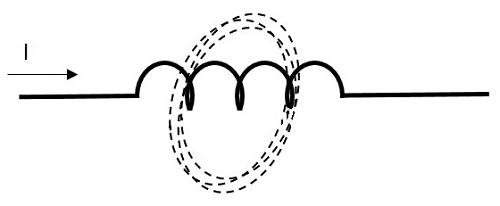
Now, here we have a varying magnetic field, which creates some current through the conductor. But this current is produced such that it opposes the main current, which has produced the magnetic field.
If this current is named as Im which means the current produced due to the magnetic field and the magnetic field is indicated by β, the following figure indicates it.
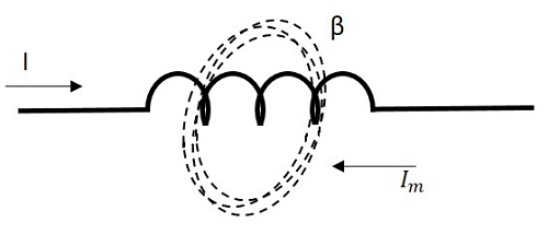
This opposing current gains strength with the varying magnetic field, which gains energy by the input supply frequency. Hence as the input current becomes more and more AC with high frequency, the resulting opposing current also gains its strength in opposite direction to the very cause producing it. Now, this opposing current, tries to stop the high frequency AC to pass through the inductor, which means blocking of AC.
Basic Electronics - Inductance
The property of an inductor to get the voltage induced by the change of current flow, is defined as Inductance. Inductance is the ratio of voltage to the rate of change of current.
The rate of change of current produces change in the magnetic field, which induces an EMF in opposite direction to the voltage source. This property of induction of EMF is called as the Inductance.
The formula for inductance is
$$Inductance\:\:=\:\:\frac{volatge}{rate\:of\:change\:of\:current}$$
Units −
The unit of Inductance is Henry. It is indicated by L.
The inductors are mostly available in mH (milli Henry) and μH (micro Henry).
A coil is said to have an inductance of one Henry when an EMF of one volt is self-induced in the coil where the current flowing changed at a rate of one ampere per second.
Self-Inductance
If a coil is considered in which some current flows, it has some magnetic field, perpendicular to the current flow. When this current keeps on varying, the magnetic field also changes and this changing magnetic field, induces an EMF, opposite to the source voltage. This opposing EMF produced is the self-induced voltage and this method is called as self-inductance.
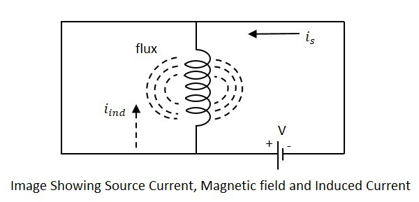
The current is in the figure indicate the source current while iind indicates the induced current. The flux represents the magnetic flux created around the coil. With the application of voltage, the current is flows and flux gets created. When the current is varies, the flux gets varied producing iind.
This induced EMF across the coil is proportional to the rate of change in current. The higher the rate of change in current the higher the value of EMF induced.
We can write the above equation as
$$E\:\:\alpha\:\:\frac{dI}{dt}$$
$$E\:\:=\:\:L\:\:\frac{dI}{dt}$$
Where,
E is the EMF produced
dI/dt indicates the rate of change of current
L indicates the co-efficient of inductance.
Self-inductance or Co-efficient of Self-inductance can be termed as
$$L\:\:=\:\:\frac{E}{\frac{dI}{dt}}$$
The actual equation is written as
$$E\:\:=\:\:-L\:\:\frac{dI}{dt}$$
The minus in the above equation indicates that the EMF is induced in opposite direction to the voltage source according to Lenzs law.
Mutual Inductance
As the current carrying coil produces some magnetic field around it, if another coil is brought near this coil, such that it is in the magnetic flux region of the primary, then the varying magnetic flux induces an EMF in the second coil. If this first coil is called as Primary coil, the second one can be called as a Secondary coil.
When the EMF is induced in the secondary coil due to the varying magnetic field of the primary coil, then such phenomenon is called as the Mutual Inductance.
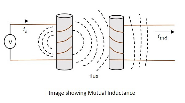
The current is in the figure indicate the source current while iind indicates the induced current. The flux represents the magnetic flux created around the coil. This spreads to the secondary coil also.
With the application of voltage, the current is flows and flux gets created. When the current is varies, the flux gets varied producing iind in the secondary coil, due to the Mutual inductance property.
The change took place like this.
$$V_{p}\:\:I_{p}\rightarrow\:\:B\:\:\rightarrow\:\:V_{s}\:\:I_{s}$$
Where,
Vp ip Indicate the Voltage and current in Primary coil respectively
B Indicates Magnetic flux
Vs is Indicate the Voltage and current in Secondary coil respectively
Mutual inductance M of the two circuits describes the amount of the voltage in the secondary induced by the changes in the current of the primary.
$$V(Secondary)\:\:=\:\:-M\frac{\Delta I}{\Delta t}$$
Where $\frac{\Delta I}{\Delta t}$ the rate of change of current with time and M is the co-efficient of Mutual inductance. The minus sign indicates the direction of current being opposite to the source.
Units −
The units of Mutual inductance is
$$volt\:\:=\:\:M\frac{amps}{sec}$$
(From the above equation)
$$M\:\:=\:\:\frac{volt.\:sec}{amp}$$
$$=\:\:Henry(H)$$
Depending upon the number of turns of the primary and the secondary coils, the magnetic flux linkage and the amount of induced EMF varies. The number of turns in primary is denoted by N1 and secondary by N2. The co-efficient of coupling is the term that specifies the mutual inductance of the two coils.
Factors affecting Inductance
There are a few factors that affect the performance of an inductor. The major ones are discussed below.
Length of the coil
The length of the inductor coil is inversely proportional to the inductance of the coil. If the length of the coil is more, the inductance offered by that inductor gets less and vice versa.
Cross sectional area of the coil
The cross sectional area of the coil is directly proportional to the inductance of the coil. The higher the area of the coil, the higher the inductance will be.
Number of turns
With the number of turns, the coil affects the inductance directly. The value of inductance gets square to the number of turns the coil has. Hence the higher the number of turns, square of it will be the value of inductance of the coil.
Permeability of the core
The permeability (μ) of the core material of inductor indicates the support the core provides for the formation of a magnetic field within itself. The higher the permeability of the core material, the higher will be the inductance.
Coefficient of Coupling
This is an important factor to be known for calculating Mutual inductance of two coils. Let us consider two nearby coils of N1 and N2 turns respectively.
The current through first coil i1 produces some flux Ψ1. The amount of magnetic flux linkages is understood by weber-turns.
Let the amount of magnetic flux linkage to the second coil, due to unit current of i1 be
$$\frac{N_{2}\varphi_{1}}{i_{1}}$$
This can be understood as the Co-efficient of Mutual inductance, which means
$$M\:\:=\:\:\frac{N_{2}\varphi_{1}}{i_{1}}$$
Hence the Co-efficient of Mutual inductance between two coils or circuits is understood as the weber-turns in one coil due to 1A of current in the other coil.
If the self-inductance of first coil is L1, then
$$L_{1}i_{1}\:\:=\:\:{N_{1}\varphi_{1}}\:\:=>\:\:\frac{L_{1}}{N_{1}}\:\:\frac{\varphi_{1}}{i_{1}}$$
$$M\:\:=\:\:\frac{N_{2}L_{1}}{N_{1}}$$
Similarly, coefficient of mutual inductance due to current i2 in the second coil is
$$M\:\:=\:\:\frac{N_{1}\varphi_{2}}{i_{2}}\:\dotsm\:\dotsm\:\dotsm\:\dotsm\:\:1$$
If self-inductance of second coil is L2
$$L_{2}i_{2}\:\:=\:\:N_{2}\varphi_{2}$$
$$\frac{L_{2}}{N_{2}}\:\:=\:\:\frac{\varphi_{2}}{i_{2}}$$
Therefore,
$$M\:\:=\:\:\frac{N_{1}L_{2}}{N_{2}}\:\dotsm\:\dotsm\:\dotsm\:\dotsm\:\:2$$
Multiplying 1 and 2, we get
$$M\:\:\times\:\:M=\:\:\frac{N_{2}L_{1}}{N_{1}}\:\:\times\:\:\frac{N_{1}L_{2}}{N_{2}}$$
$$M^{2}\:\:=\:\:L_{1}L_{2}\:\:=>\:\:M\:\:=\:\:\sqrt{L_{1}L_{2}}$$
The above equation holds true when the whole changing flux of primary coil links with the secondary coil, which is an ideal case. But in practice, it is not the case. Hence, we can write as
$$M\:\:\neq\:\:\sqrt{L_{1}L_{2}}$$
$$and \frac{M}{\sqrt{L_{1}L_{2}}}\:\:=\:\:K\:\:\neq\:\:1$$
Where K is known as the coefficient of coupling.
The Coefficient of coupling K can be defined as the ratio of actual coefficient of mutual inductance to the ideal (maximum) coefficient of mutual inductance.
If the value of k is near to unity, then the coils are said to be tightly coupled and if the value of k = 0, then the coils are said to be loosely coupled.
Applications of Inductors
There are many applications of Inductors, such as −
Inductors are used in filter circuits to sense high-frequency components and suppress noise signals
To isolate the circuit from unwanted HF signals.
Inductors are used in electrical circuits to form a transformer and isolate the circuits from spikes.
Inductors are also used in motors.
Circuit Connections in Inductors
An Inductor when connected in a circuit, that connection can be either series or parallel. Let us now know what will happen to the total current, voltage and resistance values if they are connected in series as well, when connected in parallel.
Inductors in Series
Let us observe what happens, when few inductors are connected in Series. Let us consider three resistors with different values, as shown in the figure below.
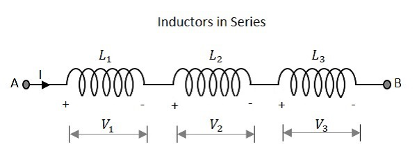
Inductance
The total inductance of a circuit having series inductors is equal to the sum of the individual inductances. Total inductance value of the network given above is
$$L_{T}\:\:=\:\:L_{1}\:\:+\:\:L_{2}\:\:+\:\:L_{3}$$
Where L1 is the inductance of 1st resistor, L2 is the inductance of 2nd resistor and L3 is the inductance of 3rd resistor in the above network.
Voltage
The total voltage that appears across a series inductors network is the addition of voltage drops at each individual inductances.
Total voltage that appears across the circuit
$$V\:\:=\:\:V_{1}\:\:+\:\:V_{2}\:\:+\:\:V_{3}$$
Where V1 is the voltage drop across 1st inductor, V2 is the voltage drop across 2nd inductor and V3 is the voltage drop across 3rd inductor in the above network.
Current
The total amount of Current that flows through a set of inductors connected in series is the same at all the points throughout the network.
The Current through the network
$$I\:\:=\:\:I_{1}\:\:=\:\:I_{2}\:\:=\:\:I_{3}$$
Where I1 is the current through the 1st inductor, I2 is the current through the 2nd inductor and I3 is the current through the 3rd inductor in the above network.
Inductors in Parallel
Let us observe what happens, when few resistors are connected in Parallel. Let us consider three resistors with different values, as shown in the figure below.
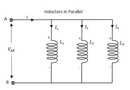
Inductance
The total inductance of a circuit having Parallel resistors is calculated differently from the series inductor network method. Here, the reciprocal (1/R) value of individual inductances are added with the inverse of algebraic sum to get the total inductance value.
Total inductance value of the network is
$$\frac{1}{L_{T}}\:\:=\:\:\frac{1}{L_{1}}\:\:+\:\:\frac{1}{L_{2}}\:\:+\:\:\frac{1}{L_{3}}$$
Where L1 is the inductance of 1st inductor, L2 is the inductance of 2nd inductor and L3 is the inductance of 3rd inductor in the above network.
From the method we have for calculating parallel inductance, we can derive a simple equation for two-inductor parallel network. It is
$$L_{T}\:\:=\:\:\frac{L_{1}\:\:\times\:\: L_{2}}{L_{1}\:\:+\:\: L_{2}}$$
Voltage
The total voltage that appears across a Parallel inductors network is same as the voltage drops at each individual inductances.
The Voltage that appears across the circuit
$$V\:\:=\:\:V_{1}\:\:=\:\:V_{2}\:\:=\:\:V_{3}$$
Where V1 is the voltage drop across 1st inductor, V2 is the voltage drop across 2nd inductor and V3 is the voltage drop across 3rd inductor in the above network. Hence the voltage is same at all the points of a parallel inductor network.
Current
The total amount of current entering a Parallel inductive network is the sum of all individual currents flowing in all the Parallel branches. The inductance value of each branch determines the value of current that flows through it.
The total Current through the network is
$$I\:\:=\:\:I_{1}\:\:+\:\:I_{2}\:\:+\:\:I_{3}$$
Where I1 is the current through the 1st inductor, I2 is the current through the 2nd inductor and I3 is the current through the 3rd inductor in the above network.
Hence the sum of individual currents in different branches obtain the total current in a parallel network.
Inductive Reactance
Inductive Reactance is the opposition offered by an inductor to the alternating current flow, or simply AC current. An inductor has the property of resisting the change in the flow of current and hence it shows some opposition which can be termed as reactance, as the frequency of the input current should also be considered along with the resistance it offers.
Indication − XL
Units − Ohms
Symbol − Ω
In a purely inductive circuit, the current IL lags the applied voltage by 90. Inductive reactance is calculated by,
$$X_{L}\:\:=\:\:2\pi fL$$
Where f is the frequency of the signal. Hence inductive reactance is a function of frequency and inductance.
Basic Electronics - Types of Inductors
Inductors are available in different shapes and has different uses. Their sizes vary depending upon the material used to manufacture them. The main classification is done as fixed and variable inductors. An inductor of few Henries may be in a dumbbell shape at the size of a simple resistor. A fixed inductor always has silver as its first color in color coding.
The Core of the Inductor is its heart. There are many types of Inductors according to the core material used. Let us have a look at a few of them.
Air-core Inductor
The commonly seen inductor, with a simple winding is this air-Core Inductor. This has nothing but air as the core material. The non-magnetic materials like plastic and ceramic are also used as core materials and they also come under this air-core Inductors. The following image shows various air-core inductors.
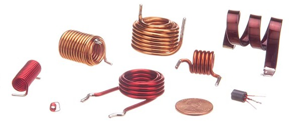
These Inductors offer a minimum signal loss at the applications having a very high magnetic field strength. Also, there exists no core losses as there is no solid core material.
Iron-Core Inductor
These Inductors have Ferromagnetic materials, such as ferrite or iron, as the core material. The usage of such core materials helps in the increase of inductance, due to their high magnetic permeability. Permeability measures the ability of supporting the formation of magnetic fields within the materials. The following image shows how an Iron-core Inductor looks like −
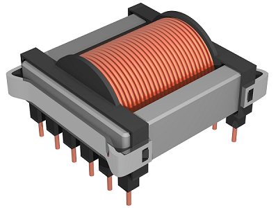
The inductors that have ferromagnetic core materials just like these, suffer from core losses and energy losses at high frequencies. These Inductors are used in the manufacture of few types of transformers.
Toroidal Inductors
These Inductors have a magnetic material as the core substance to which the wire is wound. These are in circular ring shape, just as shown in the following figure.
The main advantage of this type of inductors is that, due to the circular shape, symmetry is achieved in the whole shape of the inductor, due to which there are minimum losses in the magnetic flux. These inductors are mostly used in AC circuit applications.
Laminated Core Inductors
These are the inductors that have laminated thin steel sheets, such as stacks, as the core materials. Usually for an inductor, if the loop area is increased for the current to travel, the energy losses will be more. Whereas, in these laminated core Inductors, thin steel sheets of stacks are helpful in blocking the eddy currents, which minimize the loop action.
The following figure shows an image of a laminated core inductor.
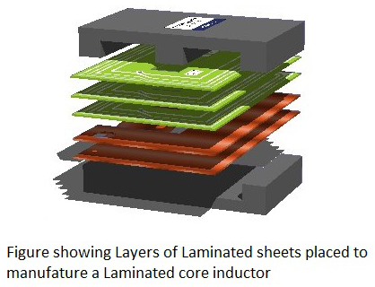
The main advantage of these inductors is minimizing the energy loss with its construction. These laminated core inductors are mostly used in the manufacture of transformers.
Powdered Iron Core Inductors
As the name implies, the core of these inductors have magnetic materials with some air gaps in it. But this kind of construction provides an advantage to the core, to store high level of energy compared with the other types. The following figure shows an image of a Powdered Iron core Inductor.
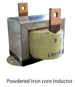
These inductors provide very low eddy current losses and hysteresis losses. These are available at lowest prices and have very good inductance stability.
Basic Electronics - RF Inductors
RF inductors are the radio frequency inductors, which are used at high resonant frequencies. These can be multilayered coil inductor or a thin film coated ceramic inductor or some wire wound ceramic inductor. The following figure represents few RF inductors.
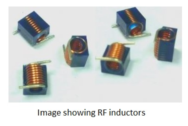
These inductors are characterized by low current rating and high electrical resistance. But as the high frequencies are used here, the wire resistance increases. Also, few effects come into picture because of these high resonant radio frequencies. Let us have a look at them.
Skin Effect
At high frequencies, the alternating current has a tendency of unequal distribution of current through the conductor. The electric current flows highly at the surface of the conductor than at its center. It gets its energy concentrated in the skin of the conductor, leaving the deep core of the conductor, as shown in the following figure.
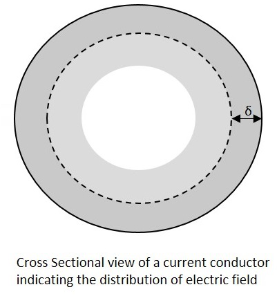
As the energy gets concentrated at the skin of the conductor, this effect is called as the Skin Effect. Actually this skin effect is caused due to the eddy currents which are produced by the changing Magnetic field, resulting from alternating current. Now-a-days, the conductors carrying higher frequencies are made in the form of tube shape, in order to reduce the weight and cost of the conductors.
Proximity Effect
Along with the above one, this is another effect, which is observed here. Proximity effect is the one which increases the resistance of the wire at high frequencies. Proximity is the word which says that the effect will be on adjacent wires. The following figure shows the concentration of current on the edges of the adjacent cables.
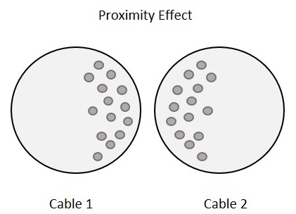
Each turn has some magnetic field which induces eddy currents in the wire that causes the current to be focused on the side of the adjacent wire. With this effect, the effective cross sectional area of the wire gets reduced and its resistance gets increased.
Parasitic Capacitance
Usually, an inductor internally contains a resistor in series (wire resistance) and a capacitor in shunt (parasitic capacitance). Each turn of winding has slightly different potential, in an inductor. The following figure shows the capacitance effect in an inductor.
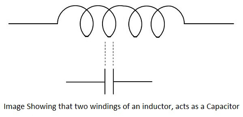
The two conductors that present in each turn, act as capacitor plates with air as dielectric. A capacitance called as Parasitic Capacitance exists here. In order to avoid this in certain applications, the windings are made far to each other.
As the frequency increases, the impedance of the parasitic capacitance decreases and the impedance of inductor increases. Hence the inductor tends to behave like a capacitor.
Dielectric losses
The current through the conductor of an inductor makes the molecules of the insulators exert energy in the form of heat. The higher the frequency, the greater the heat dissipation will be.
Chokes
Inductors are also called as chokes. An Inductor blocks AC components and sends DC components through it. Hence as it chokes or stops AC, an inductor can simply be termed as a Choke.
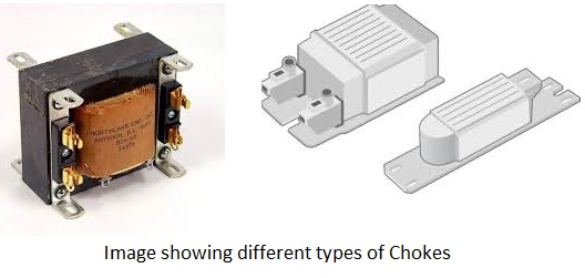
A coil of insulated wire is often wound on a magnetic core to form a choke. As the signal frequency increases, the impedance of the choke increases. Due to its reactance, it can limit the amount AC through it. Even though, practically some amount of AC passes through it due to its low electrical resistance. These are mostly used in tube lights and in transformers in electronic applications.
Basic Electronics - Transformers
According to the principle of Electromagnetic Induction, we have already learnt that, a varying flux can induce an EMF in a coil. By the principle of Mutual induction, when another coil is brought beside such coil, the flux induces EMF into the second coil.
Now, the coil which has the varying flux is called as the Primary Coil and the coil into which EMF is induced is called as the Secondary Coil, while the two coils together makes a unit called as a Transformer.
Transformer
A transformer has a primary coil to which input is given and a secondary coil from which the output is collected. Both of these coils are wound on a core material. Usually an insulator forms the Core of the transformer.
The following figure shows a practical transformer.
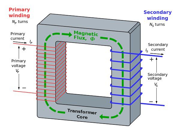
From the above figure, it is evident that few notations are common. Let us try to have a note of them. They are −
Np = Number of turns in the primary winding
Ns = Number of turns in the secondary winding
Ip = Current flowing in the primary of the transformer
Is = Current flowing in the secondary of the transformer
Vp = Voltage across the primary of the transformer
Vs = Voltage across the secondary of the transformer
Φ = Magnetic flux present around the core of the transformer.
Transformer in a Circuit
The following figure shows how a transformer is represented in a circuit. The primary winding, the secondary winding and the core of the transformer are also represented in the following figure.
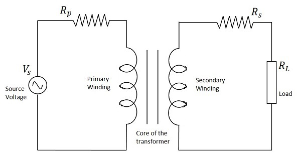
Hence, when a transformer is connected in a circuit, the input supply is given to the primary coil so that it produces varying magnetic flux with this power supply and that flux is induced into the secondary coil of the transformer, which produces the varying EMF of the varying flux. As the flux should be varying, for the transfer of EMF from primary to secondary, a transformer always works on alternating current AC.
Step-up and Step-down
Depending upon the number of turns in the secondary winding, the transformer can be called as a Step up or a Step down transformer.
The main point to be noted here is that, there will not be any difference in the primary and secondary power of the transformer. Accordingly, if the voltage is high at secondary, then low current is drawn to make the power stable. As well, if the voltage in the secondary is low, then high current is drawn so as the power must be same as the primary side.
Step Up
When the secondary winding has more number of turns than the primary winding, then the transformer is said to be a Step-up transformer. Here the induced EMF is greater than the input signal.
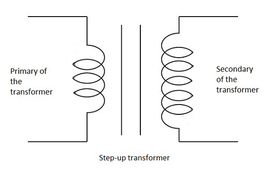
Step Down
When the secondary winding has lesser number of turns than the primary winding, then the transformer is said to be a Step-down transformer. Here the induced EMF is lesser than the input signal.
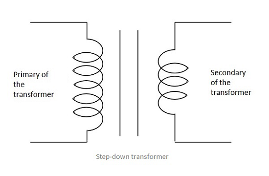
Turns Ratio
As the number of turns of primary and secondary windings affect the voltage ratings, it is important to maintain a ratio between the turns so as to have an idea regarding the voltages induced.
The ratio of number of turns in the primary coil to the number of turns in the secondary coil is called as the turns ratio or the ratio of transformation. The turns ratio is usually denoted by N.
$$N\:\:=\:\:Turns\:ratio\:\:=\:\:\frac{Number\:of\:turns\:on\:Primary}{Number\:of\:turns\:on\:Secondary}\:\:=\:\:\frac{N_{p}}{N_{s}}$$
The ratio of the primary to the secondary, the ratio of the input to the output, and the turns ratio of any given transformer will be the same as its voltage ratio. Hence this can be written as
$$\frac{N_{p}}{N_{s}}\:\:=\:\:\frac{V_{p}}{V_{s}}\:\:=\:\:N\:\:=\:\:Turns\:ratio$$
The turns ratio also states whether the transformer is a step-up or a step-down transformer. For example, a turns ratio of 1:3 states that the transformer is a step-up and the ratio 3:1 states that it is a step-down transformer.
Basic Electronics - Types of Transformers
Coming to the classification of transformers, there are many types depending upon the core used, windings used, place and type of usage, voltage levels etc.
Single and three phase transformers
According to the supply used, the transformers are mainly classified as Single phase and three phase transformers.
A normal transformer is a single phase transformer. It has a primary and a secondary winding and it is operated to either decrease or increase the secondary voltage.
For a three phase transformer, three primary windings are connected together and three secondary windings are connected together.
A single three phase transformer is preferred to three single phase transformers so as to get good efficiency, where it occupies less space at low cost. But due to the transportation problem of heavy equipment, single phase transformers are used in most cases.
Another classification of these transformers is Core and Shell type.
In Shell type, the windings are positioned on a single leg surrounded by the core.
In Core type, they are wounded on different legs.
The difference is well known by having a look at the following figure.
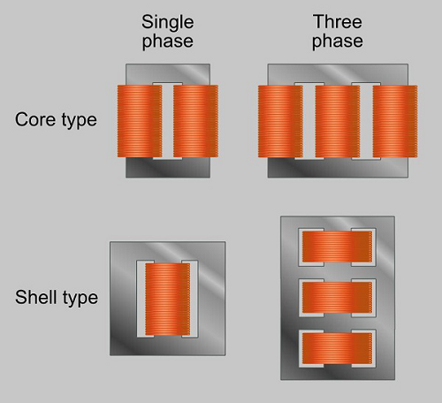
The classification of transformers can also be done depending upon the type of core material used. These are actually RF transformers, which contain many types such as Air-core transformers, Ferrite core transformers, Transmission line transformers and Balun transformers. Balun transformers are used in RF receiver systems. The main types are the air core and iron core transformers.
Air-core Transformer
This is a core type transformer in which the windings are wound on a non-magnetic strip. The magnetic flux linkages are made through air as core between the primary and secondary. The following image shows an air-core transformer.
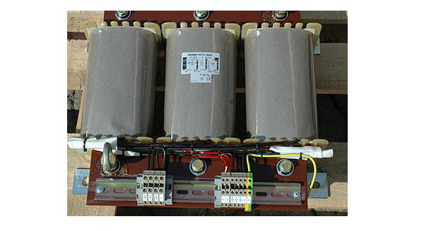
Advantages
- The hysteresis and eddy current losses are low in these Air core transformers.
- Noise production is low.
Disadvantages
- The reluctance is high in Air core transformers.
- Mutual inductance is low in Air core compared to Iron-core transformers.
Applications
- Audio frequency transformers.
- High frequency radio transmissions.
Iron Core Transformers
This is a core type transformer in which the windings are wound on an iron core. The magnetic flux linkages are made strong and perfect with iron as core material. This is commonly seen in laboratories. The figure below shows an example of iron core transformer.
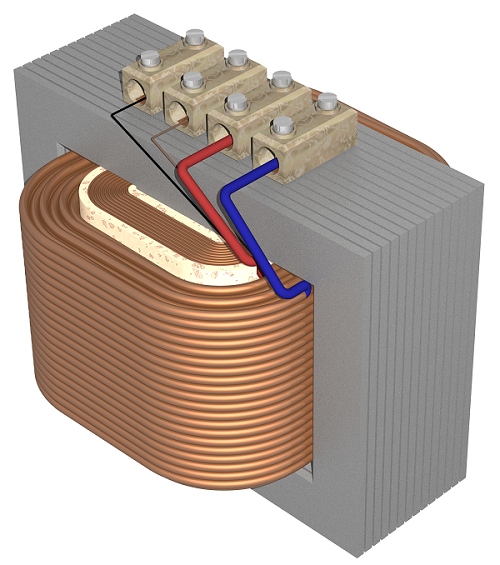
Advantages
- They have very high magnetic permeability.
- Iron core transformers has low reluctance.
- Mutual Inductance is high.
- These transformers are highly efficient.
Disadvantages
- These are a bit noisy compared to Air core transformers.
- The hysteresis and eddy current losses are a bit more than Air core transformers.
Applications
- As isolation transformers.
- High frequency radio transmissions.
The transformers are also classified according to the type of core they use. Some transformers use the core immersed in oil. This oil is cooled from outside by various methods. Such transformers are named as Wet core transformers, while the others such as ferrite core transformers, laminated core transformers, toroidal core transformers and cast resin transformers are Dry core transformers.
Based on the type of winding technique, we have another transformer which is very popular named as the Auto transformer.
Auto Transformer
This is type of transformer which is mostly seen in our electrical laboratories. This auto transformer is an improved version of the original transformer. A single winding is taken to which both the sides are connected to power and the ground. Another variable tapping is made by whose movement secondary of the transformer is formed.
The following figure shows the circuit of an auto-transformer.
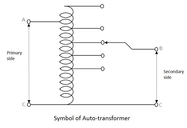
As shown in the figure, a single winding provides both primary and secondary in a transformer. Various tapping of secondary winding are drawn to select various voltage levels at the secondary side.
The primary winding as shown above is from A to C and the secondary winding is from B to C whereas the variable arm B is varied to get the required voltage levels. A practical auto transformer looks like the figure below.
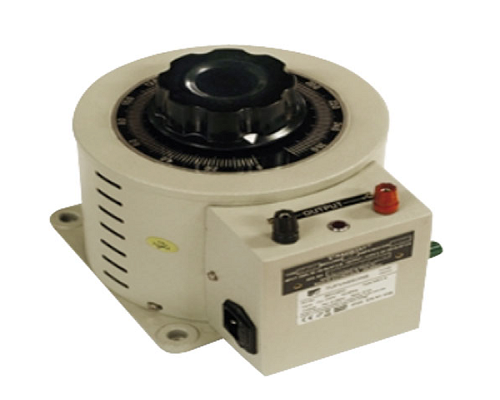
By rotating the shaft above, the secondary voltage is adjusted to different voltage levels. If the voltage applied across the points A and C is V1, then the voltage per turn in this winding will be
$$Voltage\:per\:turn\:\:=\:\:\frac{V_{1}}{N_{1}}$$
Now, the voltage across the points B and C will be
$$V_{2}\:\:=\:\:\frac{V_{1}}{N_{1}}\:\:\times\:\:N_{2}$$
$$\frac{V_{2}}{V_{1}}\:\:=\:\:\frac{N_{2}}{N_{1}}\:\:=\:\:constant\:(say\:K)$$
This constant is nothing but the turns ratio or voltage ratio of the auto transformer.
Transformers based on Usage
There are transformers which are classified depending upon the applications they have. Many of these transformers are large and bulky. Most of them are used by the Electricity department.
Power Transformers
The Power transformers are used in high power transfer applications for both step-up and step-down applications, where the operating voltages are more than 33KV generally rated above 200MVA. The flux density is much higher for them.
All the transformers that are used for power control applications such as laminated core transformers, toroidal transformers, variable auto transformers, polyphaser transformers, stray leakage transformers come under this category.
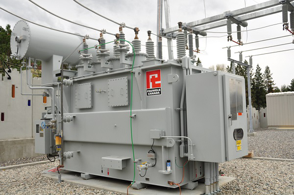
These are usually big in size depending upon the power handling capacity and its application. These transformers are available in three phase or single phase type. As these transformers are bulky, they are placed in large open area. These transformers tend to provide 100% efficiency in full load applications.
Advantages
- They have high insulation level.
- Noise is low.
- They are highly efficient.
- High voltage rated ones to handle high power applications.
Applications
- They are used in power generation systems.
- They are used in transmission sub stations.
Measurement Transformers
The Measurement transformers are used for measuring high voltage and high currents. These are mostly helpful in isolating the circuits from them. Usually, the Primary of a transformer is connected with high inputs of voltages and currents whereas Secondary of the transformer is connected to some relay or circuit which has to be provided some isolation.
These are mainly of two types, Current transformers and Voltage transformers. Let us have a look at each of them.
Current Transformer
The Current transformers provide current in the secondary circuit proportional to the current in the primary circuit. These are used in protective relays and for measurement purposes.
A single turn primary winding is passed through a well-insulated toroidal core transformer which is wounded with many turns, which makes a Current Transformer. This is always connected in series.
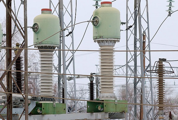
The secondary winding can be designed to provide single output or it may have several tapping for different values. Care must be taken that the secondary winding is connected to its load having low impedance, while current flows in primary. This is to avoid sudden high voltages in open circuited secondary which might permanently damage the accuracy of the transformer.
Voltage Transformers
The Voltage Transformers provide voltage in the secondary circuit proportional to the voltage in the primary circuit. These transformers are also called as Potential Transformers. These are connected in parallel to the circuit.
The primary of this transformer may have phase to phase connections but the secondary will have one terminal to ground. The figure below shows an image of a voltage transformer.
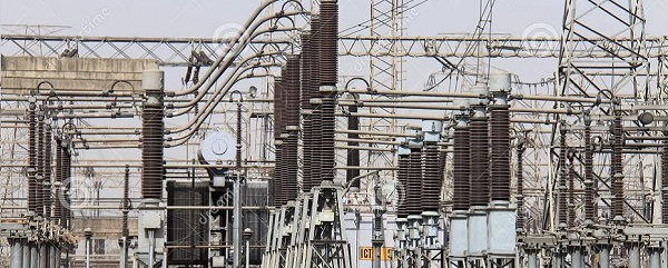
There are three main types of a voltage transformers. They are
Electromagnetic − uses a wire wound transformer having good flux linkages.
Capacitor − uses a capacitor with potential divider network.
Optical − makes use of electrical properties of optical materials.
The voltage transformers are used in protective relays and for measurement purposes and also for phasor phase shift isolation.
Protection Transformers
These transformers are very accurate than measuring transformers, as these are used only to protect the circuits from high voltages and currents. The primary of these transformers are connected with high inputs whereas the secondary of the transformer keeps the circuit or relay, isolated from the sudden spikes or surges which might damage the circuit.
Distribution Transformers
The Distribution transformers are used for distribution of electrical energy at end-user level. The operating voltages are around 33KV for industrial purposes and 440v-220v for domestic purposes. These are generally rated below 200MVA.
The large three phase auto transformers used in power distribution and the oil-cooled transformers also come under this category. The figure below shows an image of a distribution transformer.
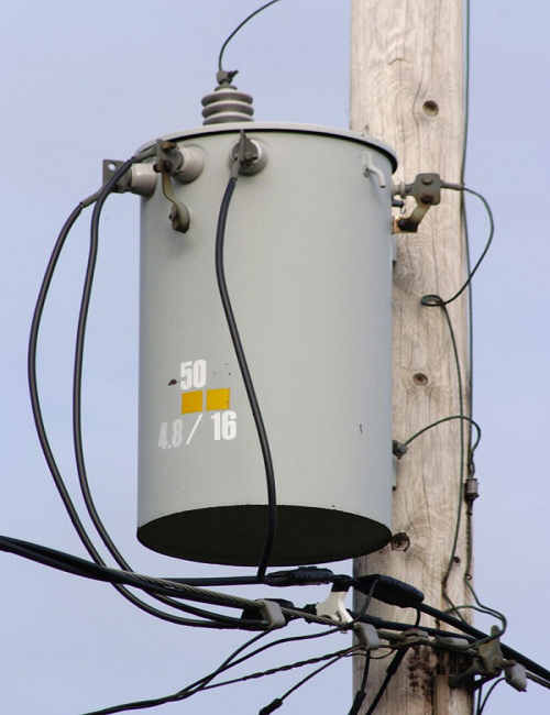
These transformers are usually smaller in size compared to power transformers. These transformers are placed in open but are not fully loaded like power transformers.
Advantages
- They are small in size.
- They are easy to install.
- These transformers have low magnetic losses.
Disadvantages
- These transformers have low efficiency.
- They are not fully-loaded.
Applications
They are used for distributing electricity in various areas like houses, farm yards, lands, railways, wind farms etc.
Basic Electronics - Transformer Efficiency
When the Primary of a transformer has some voltage induced, then the magnetic flux created in the primary is induced into the secondary due to mutual induction, which produces some voltage into the secondary. The strength of this magnetic field builds up as the current rises from zero to maximum value which is given by $\mathbf{\frac{d\varphi}{dt}}$.
The magnetic lines of flux pass through the secondary winding. The number of turns in the secondary winding determines the voltage induced. Hence the amount of voltage induced will be determined by
$$N\frac{d\varphi}{dt}$$
Where N = number of turns in the secondary winding
The frequency of this induced voltage will be same as the frequency of primary voltage. The peak amplitude of the output voltage will be affected if the magnetic losses are high.
Induced EMF
Let us try to draw some relationship between induced EMF and number of turns in a coil.
Let us now assume that both the primary and the secondary coils has a single turn each. If one volt is applied to one turn of the primary with no losses (ideal case) the current flow and magnetic field generated induce the same one volt in the secondary. Hence voltage is same on both sides.
But the magnetic flux varies sinusoidally which means,
$$\phi\:\:=\:\:\phi_{max} \sin \omega t$$
Then the basic relationship between induced EMF and coil winding of N turns is
$$EMF\:=\:turns\:\:\times\:\:rate\:of\:change$$
$$E\:=\:N \frac{d\phi}{dt}$$
$$E\:=\:N\:\times\:\omega\:\times\: \phi_{max}\:\times\: \cos(\omega t)$$
$$E_{max}\:=\:N \omega \phi_{max}$$
$$E_{rms}\:=\:\frac{N \omega}{\sqrt{2}}\:\times\:\phi_{max}\:=\:\frac{2\pi}{\sqrt{2}}\:\times\:f\:\times\:N\:\times\:\phi_{max}$$
$$E_{rms}\:=\:4.44\:f\:N\:\phi_{max}$$
Where
f = flux frequency in Hertz = $\frac{\omega}{2\pi}$
N = number of coil windings
∅ = flux density in webers
This is known as Transformer EMF Equation.
As alternating flux produces current in the secondary coil, and this alternating flux is produced by alternating voltage, we can say that only an alternating current AC can help a transformer work. Hence a transformer doesnt work on DC.
Losses in Transformers
Any Device has few losses in practical applications. The main losses that occur in the transformers are Copper losses, Core losses and Flux leakage.
Copper Losses
Copper loss is the loss of energy, due to the heat produced by the current flow through the windings of the transformers. These are also called as I2R losses or I squared R losses as the energy lost per second increases with the square of the current through the winding and is proportional to the electrical resistance of the winding.
This can be written in an equation as
$$I_{P} R_{P}\:+\:I_{S} R_{S}$$
Where
IP = Primary Current
RP = Primary Resistance
IS = Secondary Current
RS = Secondary Resistance
Core Losses
Core Losses are also called as Iron Losses. These losses depends upon the core material used. They are of two types namely, Hysteresis and Eddy Current losses.
Hysteresis Loss − The AC induced in the form of magnetic flux keeps on fluctuating (like rise and falls) and reversing the direction according to the AC voltage induced. Some energy is lost in the core due to these random fluctuations. Such loss can be termed as Hysteresis loss.
Eddy Current Loss − While this whole process goes on, some currents are induced in the core which circulate continuously. These currents produce some loss called as Eddy Current Loss. Actually the varying magnetic field is supposed to induce current only in the secondary winding. But it induces voltages in the nearby conducting materials also, which results in this loss of energy.
Flux Leakage − Though the flux linkages are strong enough to produce the required voltage, there will be some flux which gets leaked in practical applications and hence results in the energy loss. Though this is low, this loss is also countable when it comes to high energy applications.
Power of a Transformer
When an ideal transformer is considered with no losses, the Power of the transformer will be constant, as the product when voltage V multiplied by current I is constant.
We can say that the power in the primary equals the power in the secondary as the transformer takes care of that. If the transformer, steps-up the voltage then the current is reduced and if the voltage is stepped-down, the current is increased so as to maintain the output power constant.
Hence the primary power equals the secondary power.
$$P_{Primary}\:=\:P_{Secondary}$$
$$V_{P}I_{P}\cos \phi_{P}\:=\:V_{S}I_{S}\cos \phi_{S}$$
Where ∅P = Primary phase angle and ∅S = Secondary phase angle.
Efficiency of a transformer
The amount or the intensity of Power loss in a transformer, determines the efficiency of the transformer. The efficiency can be understood in terms of power loss between primary and secondary of a transformer.
Hence, the ratio of power output of secondary winding to the power input of primary winding can be stated as the Efficiency of the transformer. This can be written as
$$Efficiency\:=\:\frac{Power\:output}{Power\:input}\:\times\:100 \%$$
Efficiency is generally denoted by η. The above given equation is valid for an ideal transformer where there will be no losses and the whole energy in the input gets transferred to the output.
Hence, if losses are considered and if the efficiency is calculated in practical conditions, the below equation is to be considered.
$$Efficiency\:=\:\frac{Power\:output}{Power\:output\:+\:Copper\:losses\:+\:Core\:losses}\:\times\:100 \%$$
Otherwise, it can also be written as
$$Efficiency\:=\:\frac{Power\:input\:-\:Losses}{Power\:input}\:\times\:100$$
$$1\:-\:\frac{Losses}{Input\:Power}\:\times\:100$$
It is to be noted that the input, output and losses are all expressed in terms of power, i.e., in Watts.
Example
Consider a transformer having input power of 12KW which is rated at 62.5 amps current having equivalent resistance of 0.425ohms. Calculate the efficiency of the transformer.
Solution −
Given data
- Input power = 12KW
- Rated current = 62.5 Amps
- Equivalent resistance = 0.425 ohms
Calculating the loss −
The copper loss at rated current is I2R = (62.5)2 (0.425) = 1660W
We have
$$Efficiency\:=\:\frac{Power\:input\:-\:Losses}{Power\:input}\:\times\:100$$
Hence,
$$\eta\:=\:\frac{12000\:-\:1660}{12000}\:\times\:100$$
$$\eta\:=\:\frac{10340}{12000}\:\times\:100$$
$$\eta\:=\:0.861\:\times\:100\:=\:86 \%$$
Hence the efficiency of the transformer is 86%.
Basic Electronics - Diodes
After having known about various components, let us focus on another important component in the field of electronics, known as a Diode. A semiconductor diode is a two terminal electronic component with a PN junction. This is also called as a Rectifier.
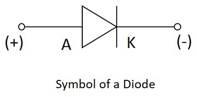
The anode which is the positive terminal of a diode is represented with A and the cathode, which is the negative terminal is represented with K. To know the anode and cathode of a practical diode, a fine line is drawn on the diode which means cathode, while the other end represents anode.
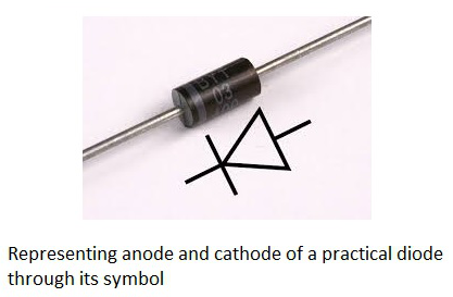
As we had already discussed about the P-type and N-type semiconductors, and the behavior of their carriers, let us now try to join these materials together to see what happens.
Formation of a Diode
If a P-type and an N-type material are brought close to each other, both of them join to form a junction, as shown in the figure below.
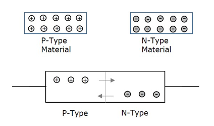
A P-type material has holes as the majority carriers and an N-type material has electrons as the majority carriers. As opposite charges attract, few holes in P-type tend to go to n-side, whereas few electrons in N-type tend to go to P-side.
As both of them travel towards the junction, holes and electrons recombine with each other to neutralize and forms ions. Now, in this junction, there exists a region where the positive and negative ions are formed, called as PN junction or junction barrier as shown in the figure.
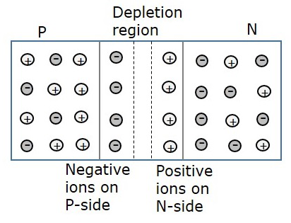
The formation of negative ions on P-side and positive ions on N-side results in the formation of a narrow charged region on either side of the PN junction. This region is now free from movable charge carriers. The ions present here have been stationary and maintain a region of space between them without any charge carriers.
As this region acts as a barrier between P and N type materials, this is also called as Barrier junction. This has another name called as Depletion region meaning it depletes both the regions. There occurs a potential difference VD due to the formation of ions, across the junction called as Potential Barrier as it prevents further movement of holes and electrons through the junction.
Biasing of a Diode
When a diode or any two-terminal component is connected in a circuit, it has two biased conditions with the given supply. They are Forward biased condition and Reverse biased condition. Let us know them in detail.
Forward Biased Condition
When a diode is connected in a circuit, with its anode to the positive terminal and cathode to the negative terminal of the supply, then such a connection is said to be forward biased condition. This kind of connection makes the circuit more and more forward biased and helps in more conduction. A diode conducts well in forward biased condition.
Reverse Biased Condition
When a diode is connected in a circuit, with its anode to the negative terminal and cathode to the positive terminal of the supply, then such a connection is said to be Reverse biased condition. This kind of connection makes the circuit more and more reverse biased and helps in minimizing and preventing the conduction. A diode cannot conduct in reverse biased condition.
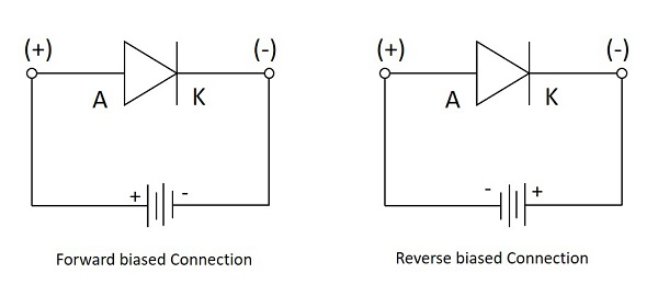
Let us now try to know what happens if a diode is connected in forward biased and in reverse biased conditions.
Working under Forward Biased
When an external voltage is applied to a diode such that it cancels the potential barrier and permits the flow of current is called as forward bias. When anode and cathode are connected to positive and negative terminals respectively, the holes in P-type and electrons in N-type tend to move across the junction, breaking the barrier. There exists a free flow of current with this, almost eliminating the barrier.
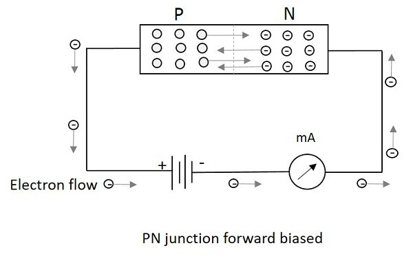
With the repulsive force provided by positive terminal to holes and by negative terminal to electrons, the recombination takes place in the junction. The supply voltage should be such high that it forces the movement of electrons and holes through the barrier and to cross it to provide forward current.
Forward Current is the current produced by the diode when operating in forward biased condition and it is indicated by If.
Working under Reverse Biased
When an external voltage is applied to a diode such that it increases the potential barrier and restricts the flow of current is called as Reverse bias. When anode and cathode are connected to negative and positive terminals respectively, the electrons are attracted towards the positive terminal and holes are attracted towards the negative terminal. Hence both will be away from the potential barrier increasing the junction resistance and preventing any electron to cross the junction.
The following figure explains this. The graph of conduction when no field is applied and when some external field is applied are also drawn.
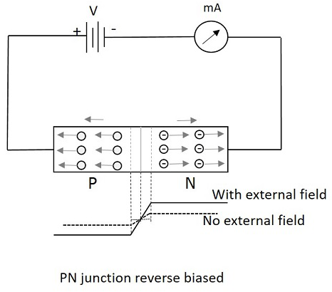
With the increasing reverse bias, the junction has few minority carriers to cross the junction. This current is normally negligible. This reverse current is almost constant when the temperature is constant. But when this reverse voltage increases further, then a point called reverse breakdown occurs, where an avalanche of current flows through the junction. This high reverse current damages the device.
Reverse current is the current produced by the diode when operating in reverse biased condition and it is indicated by Ir. Hence a diode provides high resistance path in reverse biased condition and doesnt conduct, where it provides a low resistance path in forward biased condition and conducts. Thus we can conclude that a diode is a one-way device which conducts in forward bias and acts as an insulator in reverse bias. This behavior makes it work as a rectifier, which converts AC to DC.
Peak Inverse Voltage
Peak Inverse Voltage is shortly called as PIV. It states the maximum voltage applied in reverse bias. The Peak Inverse Voltage can be defined as The maximum reverse voltage that a diode can withstand without being destroyed. Hence, this voltage is considered during reverse biased condition. It denotes how a diode can be safely operated in reverse bias.
Purpose of a Diode
A diode is used to block the electric current flow in one direction, i.e. in forward direction and to block in reverse direction. This principle of diode makes it work as a Rectifier.
For a circuit to allow the current flow in one direction but to stop in the other direction, the rectifier diode is the best choice. Thus the output will be DC removing the AC components. The circuits such as half wave and full wave rectifiers are made using diodes, which can be studied in Electronic Circuits tutorials.
A diode is also used as a Switch. It helps a faster ON and OFF for the output that should occur in a quick rate.
V - I Characteristics of a Diode
A Practical circuit arrangement for a PN junction diode is as shown in the following figure. An ammeter is connected in series and voltmeter in parallel, while the supply is controlled through a variable resistor.
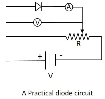
During the operation, when the diode is in forward biased condition, at some particular voltage, the potential barrier gets eliminated. Such a voltage is called as Cut-off Voltage or Knee Voltage. If the forward voltage exceeds beyond the limit, the forward current rises up exponentially and if this is done further, the device is damaged due to overheating.
The following graph shows the state of diode conduction in forward and reverse biased conditions.
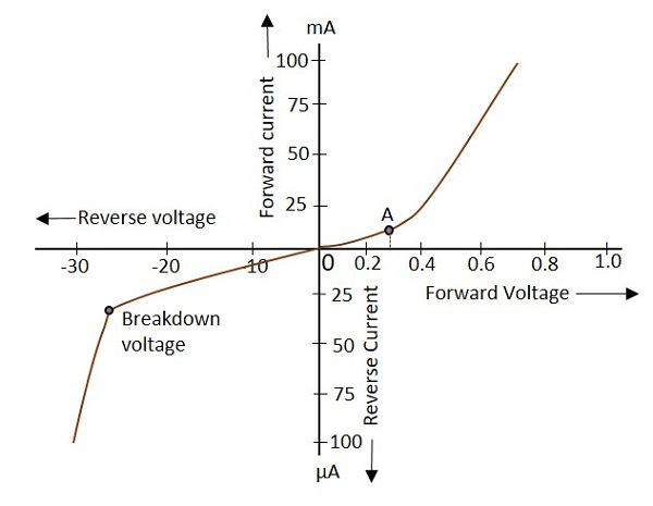
During the reverse bias, current produced through minority carriers exist known as Reverse current. As the reverse voltage increases, this reverse current increases and it suddenly breaks down at a point, resulting in the permanent destruction of the junction.
Basic Electronics - Junction Diodes
.There are many types of diodes depending upon many factors such as the frequency used, their working and construction, their applications etc. Let us go through few of them.
Junction diodes
The junction diodes are the normal PN junction diodes but differ in construction. There are three types of junction diodes, as shown in the following figure.
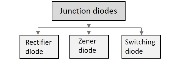
Rectifier Diode
These diodes are the normal PN junction diodes, which allow current to flow through them in only one direction and stop in the other direction. These diodes are used in rectifier circuits to convert alternating current into direct current.
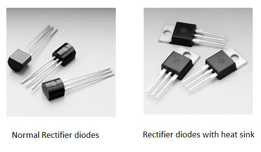
In the above figure, we can see the same rectifier diodes with a metal projection. This is added to the diode to minimize the heat distribution which might affect the diode sometimes. Such a metal projection is called as Heat sink. These help in the improvement of the diode performance and the diodes will be able to withstand high powers, without getting affected.
There are circuits such as Half wave rectifier and Full wave rectifier circuits which use these diodes. These circuits are discussed in ELECTRONIC CIRCUITS tutorial. These rectifier circuits are used in Power supply sections of many circuits where alternating input current has to be converted into direct current for that circuit applications.
Zener Diode
This is a special kind of diode which permits current flow not only in forward direction, but also in reverse direction. A normal diode, when operated in reverse bias, gets damaged if the reverse current above a certain value is passed through it. This certain value is called as the Breakdown voltage.
The breakdown voltage of a Zener diode is very low. But this diode allows the reverse current to pass through it, once this breakdown voltage is exceeded. That breakdown voltage is called as Zener Voltage. Hence there is a controlled breakdown which does not damage the diode when a reverse current above the Zener voltage passes through a Zener diode.
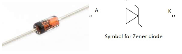
A Zener diode in its reverse bias, exhibits a controlled breakdown voltage and it allows the current flow to keep the value of voltage across that Zener diode close to the Zener breakdown voltage value. This value of Zener breakdown voltage makes any Zener diode to be chosen for certain applications.
Avalanche diode is another diode which has the similar characteristics of Zener diode. The avalanche breakdown takes place across the entire PN junction, when the voltage drop is constant and is independent of current. This avalanche diode is used for photodetection.
V-I Characteristics of a Zener diode
The V-I Characteristics of a Zener diode are common for any diode when operated in forward bias. But the reverse bias operation of a Zener diode makes it very important to consider. Let us have a look at the graph.
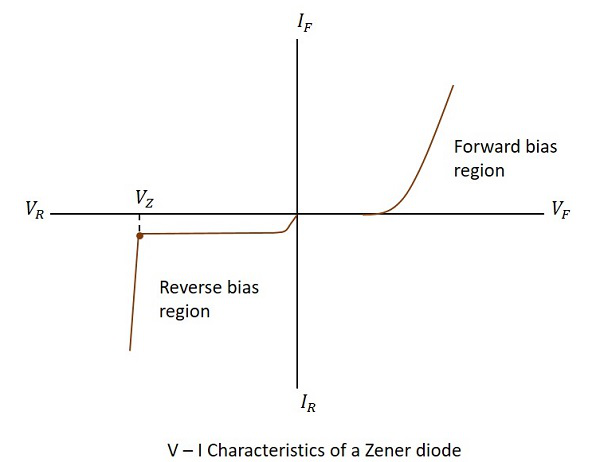
The point where the bent is shown in the reverse bias operation, is the Zener breakdown voltage, after which the diode allows high reverse currents through it. This Zener voltage is indicated by VZ. This incredible quality of Zener diode made it the most reliable one and have got many applications too.
Applications of Zener diode
This diode has many applications such as −
- It is mostly used as a Voltage Regulator.
- Provides fixed reference voltage in transistor biasing circuits.
- For peak clipping or limiting in wave shaping circuits.
- As a Surge protector in many circuits.
- For meter protection against damage from accidental applications.
Switching Diode
This is a normal single PN junction diode which is especially designed for switching purposes. This diode can exhibit two states of high and low resistance clearly which can be used alternatively.
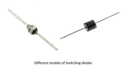
The junction capacitance of this diode is made very low so as to minimize other effects. The switching speed is made quite high. When the diode has high resistance it works as an open switch and it acts as a closed switch during low resistance. This transition occurs at a faster rate in switching diode, than in any ordinary one.
Applications of switching diode
These have many applications such as −
- Used in high-speed rectifying circuits
- Used in ring modulators
- Used in radio frequency receivers
- Used as reverse polarity protectors
- Used for both General purpose and high speed switching applications
Basic Electronics - Special Purpose Diodes
There are few diodes which are designed to serve some special purposes. There are many of such kinds like Transient voltage suppression diodes, Gold doped diodes, Super barrier diodes, Point contact diodes, Peltier diodes etc. But other than these, there are few prominent diodes, which have got many applications. Let us go through them.
Varactor Diode
A junction diode has two potentials on both sides where the depletion region can act as a dielectric. Hence there exists a capacitance. The Varactor diode is a special case diode that is operated in reverse bias, where the junction capacitance is varied.
The Varactor diode is also called as Vari Cap or Volt Cap. The following figure shows a Varactor diode connected in reverse bias.
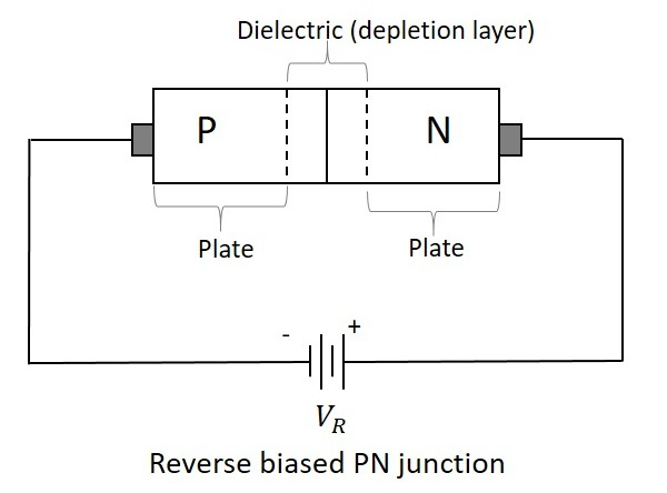
If the reverse voltage applied is increased, the width of the dielectric region increases, which reduces the junction capacitance. When the reverse voltage decreases, the width of the dielectric decreases, which increases the capacitance. If this reverse voltage is completely null, then the capacitance will be at its maximum.
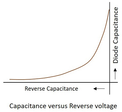
The following figure shows various symbols used for Varactor diode which represents its function.
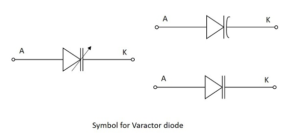
Though all diodes have this junction capacitance, the Varactor diode is mainly manufactured to make use of this effect and increase the variations in this junction capacitance.
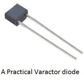
Applications of Varactor diode
This diode has many applications such as −
- It is used as a Voltage variable capacitor.
- It is used in variable LC tank circuit.
- Used as Automatic frequency control.
- Used as Frequency Modulator.
- Used as RF Phase shifter.
- Used as frequency multiplier in local oscillator circuits.
Tunnel diode
If the impurity concentration of a normal PN junction is highly increased, this Tunnel diode is formed. It is also known as Esaki diode, after its inventor.
When the impurity concentration in a diode increases, the width of depletion region decreases, extending some extra force to the charge carriers to cross the junction. When this concentration is further increased, due to less width of the depletion region and the increased energy of the charge carriers, they penetrate through the potential barrier, instead of climbing over it. This penetration can be understood as Tunneling and hence the name, Tunnel diode.
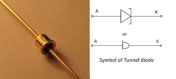
The Tunnel diodes are low power devices and should be handled with care as they easily get affected by heat and static electricity. The Tunnel diode has specific V-I characteristics which explain their working. Let us have a look at the graph below.
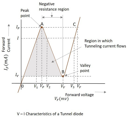
Consider the diode is in forward-biased condition. As forward voltage increases, the current increases rapidly and it increases until a peak point, called as Peak Current, denoted by IP. The voltage at this point is called as Peak Voltage, denoted by VP. This point is indicated by A in the above graph.
If the voltage is further increased beyond VP, then the current starts decreasing. It decreases until a point, called as Valley Current, denoted by IV. The voltage at this point is called as Valley Voltage, denoted by VV. This point is indicated by B in the above graph.
If the voltage is increased further, the current increases as in a normal diode. For larger values of forward voltage, the current increases further beyond.
If we consider the diode is in reverse-biased condition, then the diode acts as an excellent conductor as the reverse voltage increases. The diode here acts as in a negative resistance region.
Applications of Tunnel diode
There are many applications for tunnel diode such as −
- Used as a high-Speed Switching device
- Used as a memory storage device
- Used in Microwave oscillators
- Used in relaxation oscillators
Schottky Diode
This is a special type of diode in which a PN junction is replaced by a metal semiconductor junction. The P-type semiconductor in a normal PN junction diode is replaced by a metal and N-type material is joined to the metal. This combination has no depletion region between them. The following figure shows the Schottky diode and its symbol.
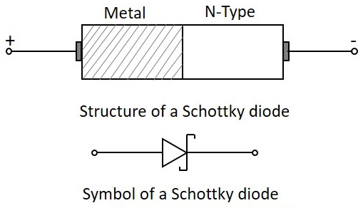
The metal used in this Schottky diode may be gold, silver, platinum or tungsten etc. As well, for the semiconductor material other than silicon, gallium arsenide is mostly used.
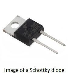
Operation
When no voltage is applied or when the circuit is unbiased, the electrons in the N-type material has lower energy level than the ones in the metal. If the diode is then forward biased, these electrons in the N-type gain some energy and move with some higher energy. Hence these electrons are called as Hot Carriers.
The following figure shows a Schottky diode connected in a circuit.
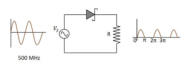
Advantages
There are many advantages of Schottky diode such as −
- It is a unipolar device and hence no reverse currents are formed.
- Its forward resistance is low.
- Voltage drops are very low.
- Rectification is fast and easy with the Schottky diode.
- There is no depletion region present and hence, no junction capacitance. So, the diode gets to OFF position quickly.
Applications
There are many applications of Schottky diode such as −
- Used as a detector diode
- Used as a Power rectifier
- Used in RF mixer circuits
- Used in power circuits
- Used as clamping diodes
Basic Electronics - Optoelectronic Diodes
These are the diodes which are operated on light. The word Opto means Light. There are types that conduction depending upon the light intensity and other types whose conduction delivers some light. Each type has got applications of their own. Let us discuss the prominent types among these ones.
Some diodes conduct according to the intensity of light falls on them. There are two main types of diodes in this category. They are Photo diodes and Solar cells.
Photo Diode
Photo diode, as the name implies, is a PN junction which works on light. The intensity of light affects the level of conduction in this diode. The photo diode has a P type material and an N-type material with an intrinsic material or a depletion region in between.
This diode is generally operated in reverse bias condition. The light when focused on the depletion region, electron-hole pairs are formed and flow of electron occurs. This conduction of electrons depends upon the intensity of light focused. The figure below shows a practical Photo diode.
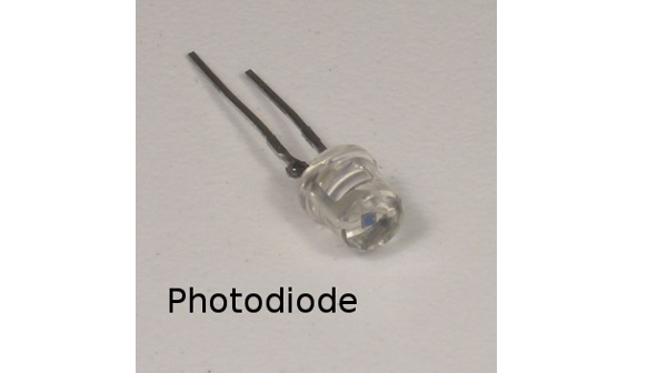
The figure below indicates the symbol for a photodiode.
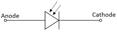
When the diode is connected in reverse bias, a small reverse saturation current flows due to thermally generated electron hole pairs. As the current in reverse bias flows due to minority carriers, the output voltage depends upon this reverse current. As the light intensity focused on the junction increases, the current flow due to minority carriers increase. The following figure shows the basic biasing arrangement of a photo diode.
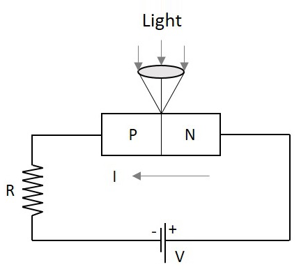
The Photo diode is encapsulated in a glass package to allow the light to fall onto it. In order to focus the light exactly on the depletion region of the diode, a lens is placed above the junction, just as illustrated above.
Even when there is no light, a small amount of current flows which is termed as Dark Current. By changing the illumination level, reverse current can be changed.
Advantages of Photo diode
Photo diode has many advantages such as −
- Low noise
- High gain
- High speed operation
- High sensitivity to light
- Low cost
- Small size
- Long lifetime
Applications of Photo diode
There are many applications for photo diode such as −
- Character detection
- Objects can be detected (visible or invisible).
- Used in circuits that require high stability and speed.
- Used in Demodulation
- Used in switching circuits
- Used in Encoders
- Used in optical communication equipment
Another diode of such a kind is Solar cell. It is termed as a cell though it is a diode. Let us get into the details.
Solar Cell
The light dependent diodes include Solar cell, which is a normal PN junction diode but has its conduction by the rush of photons which are converted into the flow of electrons. This is similar to a photo diode but it has another objective of converting maximum incident light into energy and storing it.
The figure below represents the symbol of a solar cell.
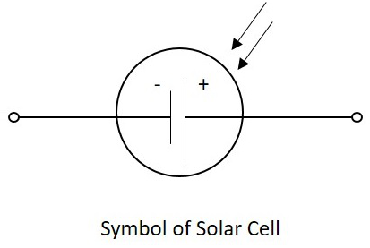
A solar cell has its name and symbol indicating storing of energy though it is a diode. The feature of extracting more energy and storing of it is concentrated in the solar cell.
Construction of a Solar cell
A PN junction diode with an intrinsic material in the deletion region is made to encapsulate in a glass. The light is made to incident on maximum area possible with thin glass on the top so as to collect maximum light with minimum resistance.
The following figure shows the construction of a Solar cell.
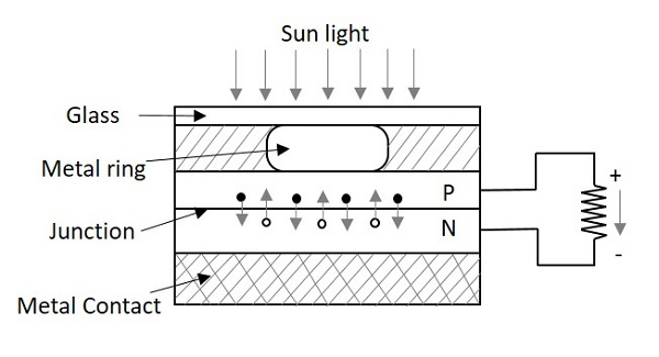
When the light is incident on the solar cell, the photons in the light collide with valence electrons. The electrons are energized to leave the parent atoms. Thus a flow of electrons is generated and this current is directly proportional to the light intensity focused onto the solar cell. This phenomenon is called as the Photo-Voltaic effect.
The following figure shows how a solar cell looks like and how a number of solar cells together are made to form a solar panel.
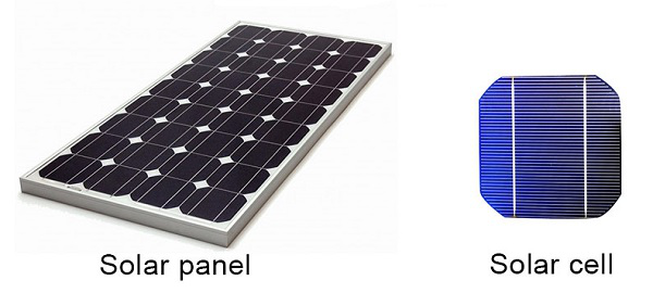
Difference between a Photo diode and Solar cell
Photo Diode works faster and concentrates on switching rather than providing more power at the output. It has a low capacitance value because of this. Also the area of incidence of light energy is lesser in Photo diode, according to its applications.
A Solar cell concentrates on delivering high output energy and storing the energy. This has high capacitance value. The operation is a bit slower than photo diode. According to the purpose of the solar cell, the area of incidence of light is larger than photo diode.
Applications of Solar Cell
There are many applications for Solar cell such as −
Science and Technology
- Used in Solar panels for Satellites
- Used in telemetry
- Used in Remote lighting systems etc.
Commercial Use
- Used in Solar panels for storage of electricity
- Used in Portable power supplies etc.
- Used in household uses such as cooking and heating using solar energy
Electronic
- Watches
- Calculators
- Electronic Toys, etc.
Some diodes emit light according to the voltage applied. There are two main types of diodes in this category. They are LEDs and Laser diodes.
LED (Light Emitting Diodes)
This one is the most popular diodes used in our daily life. This is also a normal PN junction diode except that instead of silicon and germanium, the materials like gallium arsenide, gallium arsenide phosphide are used in its construction.
The figure below shows the symbol of a Light emitting diode.
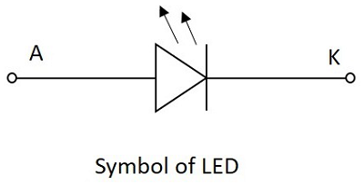
Like a normal PN junction diode, this is connected in forward bias condition so that the diode conducts. The conduction takes place in a LED when the free electrons in the conduction band combine with the holes in the valence band. This process of recombination emits light. This process is called as Electroluminescence. The color of the light emitted depends upon the gap between the energy bands.
The materials used also effect the colors like, gallium arsenide phosphide emits either red or yellow, gallium phosphide emits either red or green and gallium nitrate emits blue light. Whereas gallium arsenide emits infrared light. The LEDs for non-visible Infrared light are used mostly in remote controls.
The following figure shows a how the practical LEDs of different colors looks like.
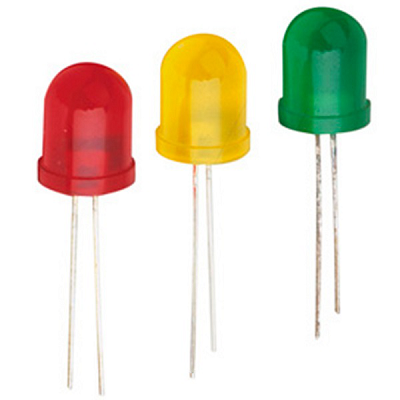
LED in the above figure has a flat side and curved side, the lead at the flat side is made shorter than the other one, so as to indicate that the shorter one is Cathode or negative terminal and the other one is Anode or the Positive terminal.
The basic structure of LED is as shown in the figure below.
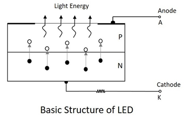
As shown in the above figure, as the electrons jump into the holes, the energy is dissipated spontaneously in the form of light. LED is a current dependent device. The output light intensity depends upon the current through the diode.
Advantages of LED
There are many advantages of LED such as −
- High efficiency
- High speed
- High reliability
- Low heat dissipation
- Larger life span
- Low cost
- Easily controlled and programmable
- High levels of brightness and intensity
- Low voltage and current requirements
- Less wiring required
- Low maintenance cost
- No UV radiation
- Instant Lighting effect
Applications of LED
There are many applications for LED such as −
In Displays
- Especially used for seven segment display
- Digital clocks
- Microwave ovens
- Traffic signaling
- Display boards in railways and public places
- Toys
In Electronic Appliances
- Stereo tuners
- Calculators
- DC power supplies
- On/Off indicators in amplifiers
- Power indicators
Commercial Use
- Infrared readable machines
- Barcode readers
- Solid state video displays
Optical Communications
- In Optical switching applications
- For Optical coupling where manual help is unavailable
- Information transfer through FOC
- Image sensing circuits
- Burglar alarms
- In Railway signaling techniques
- Door and other security control systems
Just as LED has many advantages and applications, there is another important diode called Laser diode, which also has got many advanced features and scope of future. Let us discuss about Laser diode.
Laser Diode
Laser Diode is another popular diode for its kind. This is an optical diode which emits light but with stimulated process. The name LASER implies Light Amplification by Stimulated Emission of Radiation.
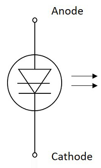
Stimulated Emission
This is a PN junction diode whose action starts when a light ray is incident on it. With a light ray, when photons get incident on an atom, the atom gets excited and it reaches an upper level which can be termed as a Higher Energy Level.
The atom when shifts from the higher energy level to a Lower Energy Level, it releases two photons which are similar in characteristics to the incident photon and are in equal phase to it. This process is called as Stimulated Emission. An atom can generally stay in this excited state for 10-8 secs of time.
So, the above process sets the principle for laser diode.
Principle of Laser Diode
Whenever a photon is incident on an atom, that atom is excited from a lower energy state to a higher energy state and two photons are released in this process. Actually, an atom can generally stay at this excited state for 10-8 secs of time. So, in order to achieve amplification, during this excited process, the atom is made to be placed in another state called Meta Stable State which is below the higher energy level and above the lower energy level.
An atom can stay in this Meta stable state for 10-3 secs. While the atom gets to the lower state from this, two photons are released. If more number of atoms are there in the excited state, prior to the photons striking the atoms, then we have the Lasing Effect.
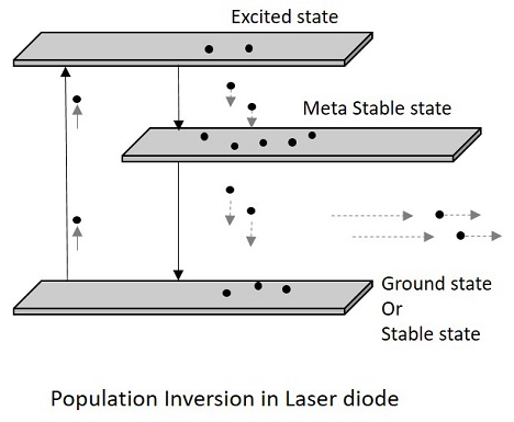
In this process, we have two terms to understand. Having more number of atoms at Meta Stable state than the lower energy state or ground state is called as Population inversion. Then energy that lets the atoms to send from a lower energy state to a higher energy state to achieve the population inversion, is called as Pumping. This is Optical pumping.
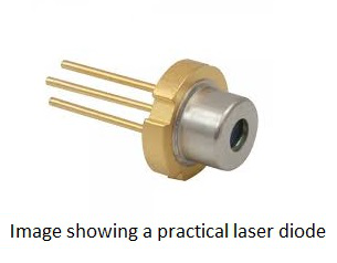
Advantages
There are many advantages of Laser diode such as −
- Power used by laser diodes is much less
- Higher ON/OFF switching speed
- More Compact
- Less expensive
- They are cheaper than laser generators
- Less chances of providing electrical shocks
Disadvantages
There are few disadvantages of Laser diode such as −
- More divergent rays and hence quality is not so good
- Their life time is less compared to LED.
- Prone to damage during unstable power supplies
Applications
There are many applications of Laser diode such as −
Used as pump-laser and seed-laser
Used in optical data storage devices
Used in laser printers and laser fax machines
Used in Laser pointers
Used in bar-code readers
They are used in DVD and CD drives
Used in HD DVD and BLU RAY technology
Has many industrial purposes such as heat treating, cladding, seam welding etc.
Has got many uses in communication technology such as data linking and transmission.
After going through all these, let us try to understand few terms.
Component
- The Components are the individual basic elements of electronics.
- They have different properties with respect to their construction.
- Every component has different applications.
Ex − Resistor, Capacitor, Diode etc.
Circuit
- A Circuit is a network of different components
- The components in the circuit altogether, survive an intended purpose.
- If a circuit has to be active, should contain a power source.
Ex − clipper and clamper circuits, amplifier circuits, relay circuits etc.
Device
A Device is an equipment that is made up of different circuits.
All circuits in the device help it function to serve its purpose.
A device can be used for measuring signals, generating signals, controlling the outcomes or protecting the circuits and so on.
Ex − CRO, Function generator etc.
Solid State devices
Previously we used to have vacuum tubes, which work on thermionic principle and are filled with vacuum inside. They were bigger in size than todays components. These vacuum tubes were replaced with semiconductor devices, which are also called as Solid state devices.
Active Devices
The devices (or precisely components) which can control the current flow can be termed as Active Devices.
- They require some input power supply to get into conduction.
- The working of these components define the behavior of the circuit.
Ex − Vacuum tubes, diodes, transistors, SCRs
Passive Devices
The devices (or precisely components) which cannot control the current flow can be termed as Passive Devices.
- They dont require input power supply to work.
- The working of these components slightly alters the circuits behavior.
Ex − Resistor, Capacitor, Inductor etc.
Doping
The process of adding of electrons or creating holes to alter the characteristics of the semiconductor material, either by making more positive or by making more negative can be understood as Doping.
The applications of diodes include many circuits starting from clipper and clamper circuits, which will be discussed in ELECTRONIC CIRCUITS tutorial.
Basic Electronics - Transistors
After having a good knowledge on the working of the diode, which is a single PN junction, let us try to connect two PN junctions which make a new component called Transistor. A Transistor is a three terminal semiconductor device that regulates current or voltage flow and acts as a switch or gate for signals.
Why Do We Need Transistors?
Suppose that you have a FM receiver which grabs the signal you want. The received signal will obviously be weak due to the disturbances it would face during its journey. Now if this signal is read as it is, you cannot get a fair output. Hence we need to amplify the signal. Amplification means increasing the signal strength.
This is just an instance. Amplification is needed wherever the signal strength has to be increased. This is done by a transistor. A transistor also acts as a switch to choose between available options. It also regulates the incoming current and voltage of the signals.
Constructional Details of a Transistor
The Transistor is a three terminal solid state device which is formed by connecting two diodes back to back. Hence it has got two PN junctions. Three terminals are drawn out of the three semiconductor materials present in it. This type of connection offers two types of transistors. They are PNP and NPN which means an N-type material between two Ptypes and the other is a P-type material between two N-types respectively.
The construction of transistors is as shown in the following figure which explains the idea discussed above.
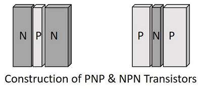
The three terminals drawn from the transistor indicate Emitter, Base and Collector terminals. They have their functionality as discussed below.
Emitter
The left hand side of the above shown structure can be understood as Emitter.
This has a moderate size and is heavily doped as its main function is to supply a number of majority carriers, i.e. either electrons or holes.
As this emits electrons, it is called as an Emitter.
This is simply indicated with the letter E.
Base
The middle material in the above figure is the Base.
This is thin and lightly doped.
Its main function is to pass the majority carriers from the emitter to the collector.
This is indicated by the letter B.
Collector
The right side material in the above figure can be understood as a Collector.
Its name implies its function of collecting the carriers.
This is a bit larger in size than emitter and base. It is moderately doped.
This is indicated by the letter C.
The symbols of PNP and NPN transistors are as shown below.
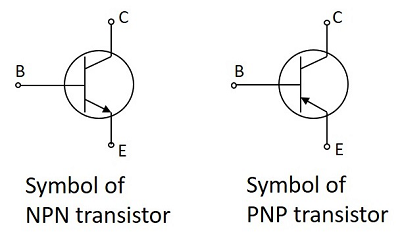
The arrow-head in the above figures indicated the emitter of a transistor. As the collector of a transistor has to dissipate much greater power, it is made large. Due to the specific functions of emitter and collector, they are not interchangeable. Hence the terminals are always to be kept in mind while using a transistor.
In a Practical transistor, there is a notch present near the emitter lead for identification. The PNP and NPN transistors can be differentiated using a Multimeter. The following figure shows how different practical transistors look like.
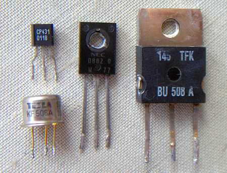
We have so far discussed the constructional details of a transistor, but to understand the operation of a transistor, first we need to know about the biasing.
Transistor Biasing
As we know that a transistor is a combination of two diodes, we have two junctions here. As one junction is between the emitter and base, that is called as Emitter-Base junction and likewise, the other is Collector-Base junction.
Biasing is controlling the operation of the circuit by providing power supply. The function of both the PN junctions is controlled by providing bias to the circuit through some dc supply. The figure below shows how a transistor is biased.
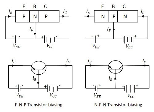
By having a look at the above figure, it is understood that
The N-type material is provided negative supply and P-type material is given positive supply to make the circuit Forward bias.
The N-type material is provided positive supply and P-type material is given negative supply to make the circuit Reverse bias.
By applying the power, the emitter base junction is always forward biased as the emitter resistance is very small. The collector base junction is reverse biased and its resistance is a bit higher. A small forward bias is sufficient at the emitter junction whereas a high reverse bias has to be applied at the collector junction.
The direction of current indicated in the circuits above, also called as the Conventional Current, is the movement of hole current which is opposite to the electron current.
Operation PNP Transistor
The operation of a PNP transistor can be explained by having a look at the following figure, in which emitter-base junction is forward biased and collector-base junction is reverse biased.
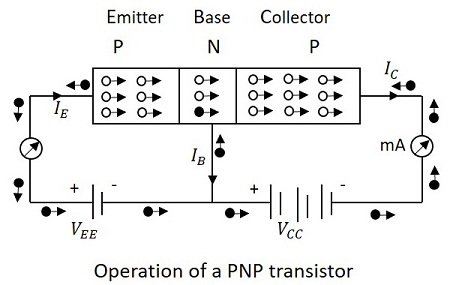
The voltage VEE provides a positive potential at the emitter which repels the holes in the P-type material and these holes cross the emitter-base junction, to reach the base region. There a very low percent of holes recombine with free electrons of N-region. This provides very low current which constitutes the base current IB. The remaining holes cross the collector-base junction, to constitute collector current IC, which is the hole current.
As a hole reaches the collector terminal, an electron from the battery negative terminal fills the space in the collector. This flow slowly increases and the electron minority current flows through the emitter, where each electron entering the positive terminal of VEE, is replaced by a hole by moving towards the emitter junction. This constitutes emitter current IE.
Hence we can understand that −
- The conduction in a PNP transistor takes place through holes.
- The collector current is slightly less than the emitter current.
- The increase or decrease in the emitter current affects the collector current.
Operation NPN Transistor
The operation of an NPN transistor can be explained by having a look at the following figure, in which emitter-base junction is forward biased and collector-base junction is reverse biased.
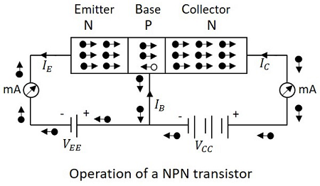
The voltage VEE provides a negative potential at the emitter which repels the electrons in the N-type material and these electrons cross the emitter-base junction, to reach the base region. There a very low percent of electrons recombine with free holes of P-region. This provides very low current which constitutes the base current IB. The remaining holes cross the collector-base junction, to constitute the collector current IC.
As an electron reaches out of the collector terminal, and enters the positive terminal of the battery, an electron from the negative terminal of the battery VEE enters the emitter region. This flow slowly increases and the electron current flows through the transistor.
Hence we can understand that −
- The conduction in a NPN transistor takes place through electrons.
- The collector current is higher than the emitter current.
- The increase or decrease in the emitter current affects the collector current.
Advantages
There are many advantages of a transistor such as −
- High voltage gain.
- Lower supply voltage is sufficient.
- Most suitable for low power applications.
- Smaller and lighter in weight.
- Mechanically stronger than vacuum tubes.
- No external heating required like vacuum tubes.
- Very suitable to integrate with resistors and diodes to produce ICs.
There are few disadvantages such as they cannot be used for high power applications due to lower power dissipation. They have lower input impedance and they are temperature dependent.
Basic Electronics - Transistor Configurations
A Transistor has 3 terminals, the emitter, the base and the collector. Using these 3 terminals the transistor can be connected in a circuit with one terminal common to both input and output in a 3 different possible configurations.
The three types of configurations are Common Base, Common Emitter and Common Collector configurations. In every configuration, the emitter junction is forward biased and the collector junction is reverse biased.
Common Base (CB) Configuration
The name itself implies that the Base terminal is taken as common terminal for both input and output of the transistor. The common base connection for both NPN and PNP transistors is as shown in the following figure.
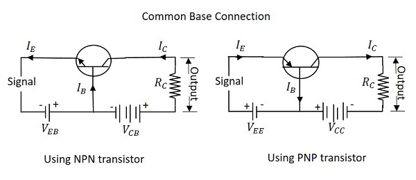
For the sake of understanding, let us consider NPN transistor in CB configuration. When the emitter voltage is applied, as it is forward biased, the electrons from the negative terminal repel the emitter electrons and current flows through the emitter and base to the collector to contribute collector current. The collector voltage VCB is kept constant throughout this.
In the CB configuration, the input current is the emitter current IE and the output current is the collector current IC.
Current Amplification Factor (α)
The ratio of change in collector current ($\Delta I_{C}$) to the change in emitter current ($\Delta I_{E}$) when collector voltage VCB is kept constant, is called as Current amplification factor. It is denoted by α.
$$\alpha\:=\:\frac{\Delta I_{C}}{\Delta I_{E}}\:\:at\:constant\:V_{CB}$$
Expression for Collector current
With the idea above, let us try to draw some expression for collector current. Along with the emitter current flowing, there is some amount of base current IB which flows through the base terminal due to electron hole recombination. As collector-base junction is reverse biased, there is another current which is flown due to minority charge carriers. This is the leakage current which can be understood as Ileakage. This is due to minority charge carriers and hence very small.
The emitter current that reaches the collector terminal is
$$\mathbf{\mathit{\alpha I_{E}}}$$
Total collector current
$$I_{C}\:=\:\alpha I_{E}\:+\:I_{leakage}$$
If the emitter-base voltage VEB = 0, even then, there flows a small leakage current, which can be termed as ICBO (collector-base current with output open).
The collector current therefore can be expressed as
$$I_{C}\:=\:\alpha I_{E}\:+\:I_{CBO}$$
$$I_{E}\:=\:I_{C}\:+\:I_{B}$$
$$I_{C}\:=\:\alpha(I_{C}\:+\:I_{B})\:+\:I_{CBO}$$
$$I_{C}(1\:-\:\alpha)\:=\:\alpha I_{B}\:+\:I_{CBO}$$
$$I_{C}\:=\:(\frac{\alpha}{1\:-\:\alpha})\: I_{B}\:+\:(\frac{I_{CBO}}{1\:-\:\alpha})$$
$$I_{C}\:=\:(\frac{\alpha}{1\:-\:\alpha})\: I_{B}\:+\:(\frac{1}{1\:-\:\alpha})I_{CBO}$$
Hence the above derived is the expression for collector current. The value of collector current depends on base current and leakage current along with the current amplification factor of that transistor in use.
Characteristics of CB configuration
This configuration provides voltage gain but no current gain.
Being VCB constant, with a small increase in the Emitter-base voltage VEB, Emitter current IE gets increased.
Emitter Current IE is independent of Collector voltage VCB.
Collector Voltage VCB can affect the collector current IC only at low voltages, when VEB is kept constant.
The input resistance ri is the ratio of change in emitter-base voltage ($\Delta{V_{EB}}$) to the change in emitter current ($\Delta{I_{E}}$) at constant collector base voltage VCB.
$$\eta\:=\:\frac{\Delta{V_{EB}}}{\Delta{I_{E}}}\:\:at\:constant\:V_{CB}$$
As the input resistance is of very low value, a small value of VEB is enough to produce a large current flow of emitter current IE.
The output resistance ro is the ratio of change in the collector base voltage ($\Delta{V_{CB}}$) to the change in collector current ($\Delta{I_{C}}$) at constant emitter current IE.
$$r_{o}\:=\:\frac{\Delta{V_{CB}}}{\Delta{I_{C}}}\: at\: constant\:l_{E}$$
As the output resistance is of very high value, a large change in VCB produces a very little change in collector current IC.
This Configuration provides good stability against increase in temperature.
The CB configuration is used for high frequency applications.
Common Emitter (CE) Configuration
The name itself implies that the Emitter terminal is taken as common terminal for both input and output of the transistor. The common emitter connection for both NPN and PNP transistors is as shown in the following figure.
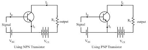
Just as in CB configuration, the emitter junction is forward biased and the collector junction is reverse biased. The flow of electrons is controlled in the same manner. The input current is the base current IB and the output current is the collector current IC here.
Base Current Amplification factor (β)
The ratio of change in collector current ($\Delta{I_{C}}$) to the change in base current ($\Delta{I_{B}}$) is known as Base Current Amplification Factor. It is denoted by β
$$\beta\:=\:\frac{\Delta{I_{C}}}{\Delta{I_{B}}}$$
Relation between β and α
Let us try to derive the relation between base current amplification factor and emitter current amplification factor.
$$\beta\:=\:\frac{\Delta{I_{C}}}{\Delta{I_{B}}}$$
$$\alpha\:=\:\frac{\Delta{I_{C}}}{\Delta{I_{E}}}$$
$$I_{E}\:=\:I_{B}\:+\:I_{C}$$
$$\Delta I_{E}\:=\:\Delta I_{B}\:+\:\Delta I_{C}$$
$$\Delta I_{B}\:=\:\Delta I_{E}\:-\:\Delta I_{C}$$
We can write
$$\beta\:=\:\frac{\Delta{I_{C}}}{\Delta I_{E}\:-\:\Delta I_{C}}$$
Dividing by $$
$$\beta\:=\:\frac{\frac{\Delta I_{C}}{\Delta I_{E}}}{\frac{\Delta I_{E}}{\Delta I_{E}}\:-\:\frac{\Delta I_{C}}{\Delta I_{E}}}$$
$$\alpha\:=\:\frac{\Delta I_{C}}{\Delta I_{E}}$$
We have
$$\alpha\:=\:\frac{\Delta I_{C}}{\Delta I_{E}}$$
Therefore,
$$\beta\:=\:\frac{\alpha}{1-\alpha}$$
From the above equation, it is evident that, as α approaches 1, β reaches infinity.
Hence, the current gain in Common Emitter connection is very high. This is the reason this circuit connection is mostly used in all transistor applications.
Expression for Collector Current
In the Common Emitter configuration, IB is the input current and IC is the output current.
We know
$$I_{E}\:=\:I_{B}\:+\:I_{C}$$
And
$$I_{C}\:=\:\alpha I_{E}\:+\:I_{CBO}$$
$$=\:\alpha (I_{B}\:+\:I_{C})\:+\:I_{CBO}$$
$$I_{C}(1\:-\:\alpha)\:=\:\alpha I_{B}\:+\:I_{CBO}$$
$$I_{C}\:=\:\frac{\alpha}{1-\alpha}I_{B}\:+\:\frac{1}{1-\alpha}\:I_{CBO}$$
If base circuit is open, i.e. if IB = 0,
The collector emitter current with base open is ICEO
$$I_{CEO}\:=\:\frac{1}{1-\alpha}\:I_{CBO}$$
Substituting the value of this in the previous equation, we get
$$I_{C}\:=\:\frac{\alpha}{1-\alpha}I_{B}\:+\:I_{CEO}$$
$$I_{C}\:=\:\beta I_{B}\:+\:I_{CEO}$$
Hence the equation for collector current is obtained.
Knee Voltage
In CE configuration, by keeping the base current IB constant, if VCE is varied, IC increases nearly to 1v of VCE and stays constant thereafter. This value of VCE up to which collector current IC changes with VCE is called the Knee Voltage. The transistors while operating in CE configuration, they are operated above this knee voltage.
Characteristics of CE Configuration
This configuration provides good current gain and voltage gain.
Keeping VCE constant, with a small increase in VBE the base current IB increases rapidly than in CB configurations.
For any value of VCE above knee voltage, IC is approximately equal to βIB.
The input resistance ri is the ratio of change in base emitter voltage ($\Delta{V_{BE}}$) to the change in base current ($\Delta{I_{B}}$) at constant collector emitter voltage VCE.
$$r_{i}\:=\:\frac{\Delta{V_{BE}}}{\Delta{I_{B}}}\:at\:constant\:V_{CE}$$
As the input resistance is of very low value, a small value of VBE is enough to produce a large current flow of base current IB.
The output resistance ro is the ratio of change in collector emitter voltage ($\Delta{V_{CE}}$) to the change in collector current ($\Delta{I_{C}}$) at constant IB.
$$r_{o}\:=\:\frac{\Delta{V_{CE}}}{\Delta{I_{C}}}\:at\:constant\:I_{B}$$
As the output resistance of CE circuit is less than that of CB circuit.
This configuration is usually used for bias stabilization methods and audio frequency applications.
Common Collector (CC) Configuration
The name itself implies that the Collector terminal is taken as common terminal for both input and output of the transistor. The common collector connection for both NPN and PNP transistors is as shown in the following figure.
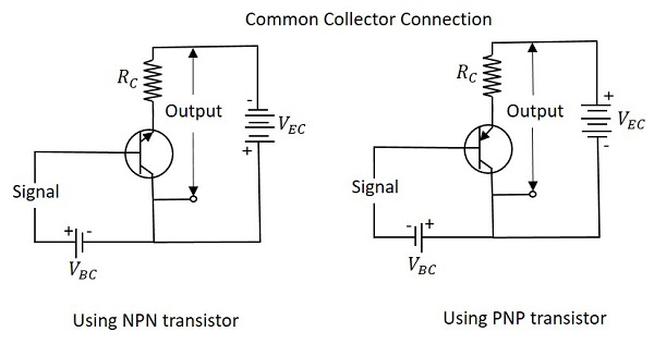
Just as in CB and CE configurations, the emitter junction is forward biased and the collector junction is reverse biased. The flow of electrons is controlled in the same manner. The input current is the base current IB and the output current is the emitter current IE here.
Current Amplification Factor (γ)
The ratio of change in emitter current ($\Delta{I_{E}}$) to the change in base current ($\Delta{I_{B}}$) is known as Current Amplification factor in common collector (CC) configuration. It is denoted by γ.
$$\gamma\:=\:\frac{\Delta{I_{E}}}{\Delta{I_{B}}}$$
The current gain in CC configuration is same as in CE configuration.
The voltage gain in CC configuration is always less than 1.
Relation between γ and α
Let us try to draw some relation between γ and α
$$\gamma\:=\:\frac{\Delta{I_{E}}}{\Delta{I_{B}}}$$
$$\alpha\:=\:\frac{\Delta{I_{C}}}{\Delta{I_{E}}}$$
$$I_{E}\:=\:I_{B}\:+\:I_{C}$$
$$\Delta I_{E}\:=\:\Delta I_{B}\:+\:\Delta I_{C}$$
$$\Delta I_{B}\:=\:\Delta I_{E}\:-\:\Delta I_{C}$$
Substituting the value of IB, we get
$$\gamma\:=\:\frac{\Delta{I_{E}}}{\Delta{I_{E}}\:-\:\Delta I_{C}}$$
Dividing by $\Delta I_{E}$
$$\gamma\:=\:\frac{\frac{\Delta I_{E}}{\Delta I_{E}}}{\frac{\Delta I_{E}}{\Delta I_{E}}\:-\:\frac{\Delta I_{C}}{\Delta I_{E}}}$$
$$\frac{1}{1\:-\:\alpha}$$
$$\gamma\:=\:\frac{1}{1\:-\:\alpha}$$
Expression for collector current
We know
$$I_{C}\:=\:\alpha I_{E}\:+\:I_{CBO}$$
$$I_{E}\:=\:I_{B}\:+\:I_{C}\:=\:I_{B}\:+\:(\alpha I_{E}\:+\:I_{CBO})$$
$$I_{E}(1\:-\:\alpha)\:=\:I_{B}\:+\:I_{CBO}$$
$$I_{E}\:=\:\frac{I_{B}}{1\:-\:\alpha}\:+\:\frac{I_{CBO}}{1\:-\:\alpha}$$
$$I_{C}\:\cong\:I_{E}\:=\:(\beta\:+\:1)I_{B}\:+\:(\beta\:+\:1)I_{CBO}$$
The above is the expression for collector current.
Characteristics of CC Configuration
This configuration provides current gain but no voltage gain.
In CC configuration, the input resistance is high and the output resistance is low.
The voltage gain provided by this circuit is less than 1.
The sum of collector current and base current equals emitter current.
The input and output signals are in phase.
This configuration works as non-inverting amplifier output.
This circuit is mostly used for impedance matching. That means, to drive a low impedance load from a high impedance source.
Transistor Regions of Operation
The DC supply is provided for the operation of a transistor. This DC supply is given to the two PN junctions of a transistor which influences the actions of majority carriers in these emitter and collector junctions.
The junctions are forward biased and reverse biased based on our requirement. Forward biased is the condition where a positive voltage is applied to the p-type and negative voltage is applied to the n-type material. Reverse biased is the condition where a positive voltage is applied to the n-type and negative voltage is applied to the p-type material.
Transistor biasing
The supply of suitable external dc voltage is called as biasing. Either forward or reverse biasing is done to the emitter and collector junctions of the transistor. These biasing methods make the transistor circuit to work in four kinds of regions such as Active region, Saturation region, Cutoff region and Inverse active region (seldom used). This is understood by having a look at the following table.
| EMITTER JUNCTION | COLLECTOR JUNCTION | REGION OF OPERATION |
|---|---|---|
| Forward biased | Forward biased | Saturation region |
| Forward biased | Reverse biased | Active region |
| Reverse biased | Forward biased | Inverse active region |
| Reverse biased | Reverse biased | Cutoff region |
Among these regions, Inverse active region, which is just the inverse of active region, is not suitable for any applications and hence not used.
Active region
This is the region in which transistors have many applications. This is also called as linear region. A transistor while in this region, acts better as an Amplifier.
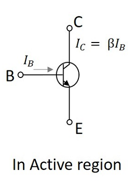
This region lies between saturation and cutoff. The transistor operates in active region when the emitter junction is forward biased and collector junction is reverse biased. In the active state, collector current is β times the base current, i.e.,
$$I_{C}\:=\:\beta I_{B}$$
Where,
$I_{C}$ = collector current
$\beta$ = current amplification factor
$I_{B}$ = base current
Saturation region
This is the region in which transistor tends to behave as a closed switch. The transistor has the effect of its collector and Emitter being shorted. The collector and Emitter currents are maximum in this mode of operation.
The figure below shows a transistor working in saturation region.
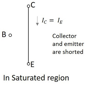
The transistor operates in saturation region when both the emitter and collector junctions are forward biased. As it is understood that, in the saturation region the transistor tends to behave as a closed switch, we can say that,
$$I_{C}\:=\:I_{E}$$
Where $I_{C}$ = collector current and $I_{E}$ = emitter current.
Cutoff region
This is the region in which transistor tends to behave as an open switch. The transistor has the effect of its collector and base being opened. The collector, emitter and base currents are all zero in this mode of operation.
The following figure shows a transistor working in cutoff region.
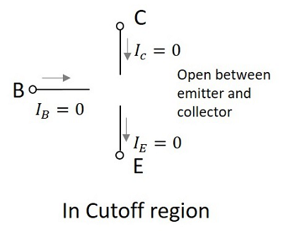
The transistor operates in cutoff region when both the emitter and collector junctions are reverse biased. As in cutoff region, the collector current, emitter current and base currents are nil, we can write as
$$I_{C}\:=\:I_{E}\:=\:I_{B}\:=\:0$$
Where $I_{C}$ = collector current, $I_{E}$ = emitter current, and $I_{B}$ = base current.
Transistor Load Line Analysis
Till now we have discussed different regions of operation for a transistor. But among all these regions, we have found that the transistor operates well in active region and hence it is also called as linear region. The outputs of the transistor are the collector current and collector voltages.
Output Characteristics
When the output characteristics of a transistor are considered, the curve looks as below for different input values.
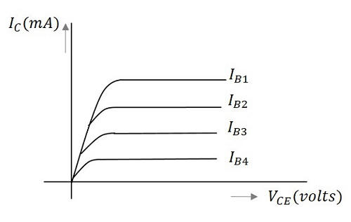
In the above figure, the output characteristics are drawn between collector current IC and collector voltage VCE for different values of base current IB. These are considered here for different input values to obtain different output curves.
Operating point
When a value for the maximum possible collector current is considered, that point will be present on the Y-axis, which is nothing but the saturation point. As well, when a value for the maximum possible collector emitter voltage is considered, that point will be present on the X-axis, which is the cutoff point.
When a line is drawn joining these two points, such a line can be called as Load line. This is called so as it symbolizes the output at the load. This line, when drawn over the output characteristic curve, makes contact at a point called as Operating point.
This operating point is also called as quiescent point or simply Q-point. There can be many such intersecting points, but the Q-point is selected in such a way that irrespective of AC signal swing, the transistor remains in active region. This can be better understood through the figure below.
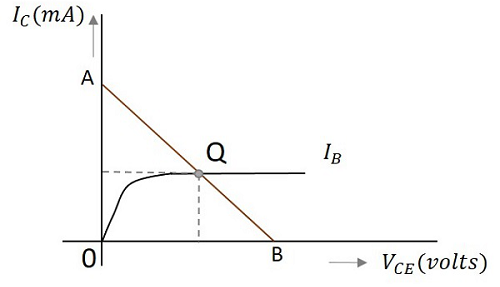
The load line has to be drawn in order to obtain the Q-point. A transistor acts as a good amplifier when it is in active region and when it is made to operate at Q-point, faithful amplification is achieved.
Faithful amplification is the process of obtaining complete portions of input signal by increasing the signal strength. This is done when AC signal is applied at its input. This is discussed in AMPLIFIERS tutorial.
DC Load line
When the transistor is given the bias and no signal is applied at its input, the load line drawn at such condition, can be understood as DC condition. Here there will be no amplification as the signal is absent. The circuit will be as shown below.
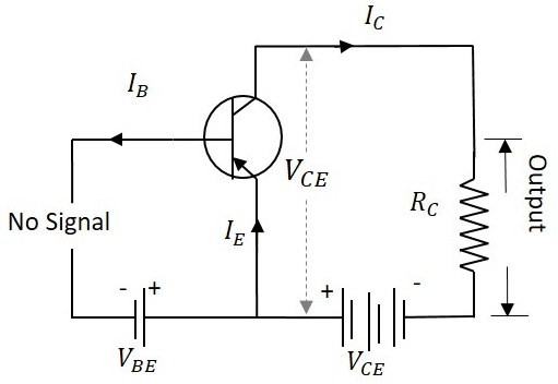
The value of collector emitter voltage at any given time will be
$$V_{CE}\:=\:V_{CC}\:-\:I_{C}R_{C}$$
As VCC and RC are fixed values, the above one is a first degree equation and hence will be a straight line on the output characteristics. This line is called as D.C. Load line. The figure below shows the DC load line.
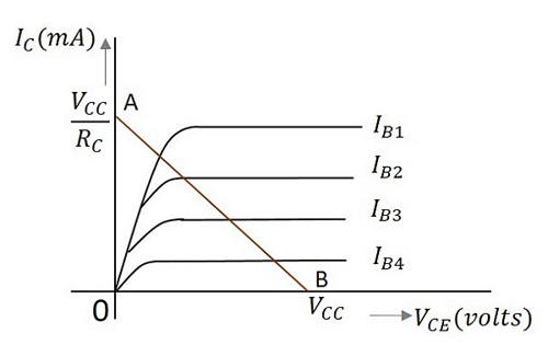
To obtain the load line, the two end points of the straight line are to be determined. Let those two points be A and B.
To obtain A
When collector emitter voltage VCE = 0, the collector current is maximum and is equal to VCC/RC. This gives the maximum value of VCE. This is shown as
$$V_{CE}\:=\:V_{CC}\:-\:I_{C}R_{C}$$
$$0\:=\:V_{CC}\:-\:I_{C}R_{C}$$
$$I_{C}\:=\:\frac{V_{CC}}{R_{C}}$$
This gives the point A (OA = VCC/RC) on collector current axis, shown in the above figure.
To obtain B
When the collector current IC = 0, then collector emitter voltage is maximum and will be equal to the VCC. This gives the maximum value of IC. This is shown as
$$V_{CE}\:=\:V_{CC}\:-\:I_{C}R_{C}$$
$$=\:V_{CC}$$
(As IC = 0)
This gives the point B, which means (OB = VCC) on the collector emitter voltage axis shown in the above figure.
Hence we got both the saturation and cutoff point determined and learnt that the load line is a straight line. So, a DC load line can be drawn.
The importance of this operating point is further understood when an AC signal is given at the input. This will be discussed in AMPLIFIERS tutorial.
Basic Electronics - Types of Transistors
There are many types of transistors in use. Each transistor is specialized in its application. The main classification is as follows.
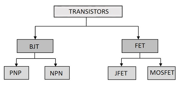
The primary transistor is the BJT and FET is the modern version of transistor. Let us have a look at the BJTs.
Bipolar Junction Transistor
A Bipolar junction transistor, shortly termed as BJT is called so as it has two PN junctions for its function. This BJT is nothing but a normal transistor. It has got two types of configurations NPN and PNP. Usually NPN transistor is preferred for the sake of convenience. The following image shows how a practical BJT looks like.
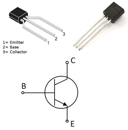
The types of BJT are NPN and PNP transistors. The NPN transistor is made by placing a ptype material between two n-type materials. The PNP transistor is made by placing an ntype material between two p-type materials.
BJT is a current controlled device. A normal transistor which we had discussed in the previous chapters come under this category. The functionality, configurations and applications are all the same.
Field Effect Transistor
An FET is a three-terminal unipolar semiconductor device. It is a voltage controlled device unlike a bipolar junction transistor. The main advantage of FET is that it has a very high input impedance, which is in the order of Mega Ohms. It has many advantages like low power consumption, low heat dissipation and FETs are highly efficient devices. The following image shows how a practical FET looks like.
The FET is a unipolar device, which means that it is made using either p-type or n-type material as main substrate. Hence the current conduction of a FET is done by either electrons or holes.
Features of FET
The following are the varied features of a Field Effect Transistor.
Unipolar − It is unipolar as either holes or electrons are responsible for conduction.
High input impedance − The input current in a FET flows due to the reverse bias. Hence it has high input impedance.
Voltage controlled device − As the output voltage of a FET is controlled by the gate input voltage, FET is called as the voltage controlled device.
Noise is low − There are no junctions present in the conduction path. Hence noise is lower than in BJTs.
Gain is characterized as transconductance. Transconductance is the ratio of change in output current to the change in input voltage.
The output impedance of a FET is low.
Advantages of FET
To prefer a FET over BJT, there should be few advantages of using FETs, rather than BJTs. Let us try to summarize the advantages of FET over BJT.
| JFET | BJT |
|---|---|
| It is an unipolar device | It is a bipolar device |
| Voltage driven device | Current driven device |
| High input impedance | Low input impedance |
| Low noise level | High noise level |
| Better thermal stability | Less thermal stability |
| Gain is characterized by transconductance | Gain is characterized by voltage gain |
Applications of FET
FET is used in circuits to reduce the loading effect.
FETs are used in many circuits such as Buffer Amplifier, Phase shift Oscillators and Voltmeters.
FET Terminals
Though FET is a three terminal device, they are not the same as BJT terminals. The three terminals of FET are Gate, Source and Drain. The Source terminal in FET is analogous to the Emitter in BJT, while Gate is analogous to Base and Drain to Collector.
The symbols of a FET for both NPN and PNP types are as shown below
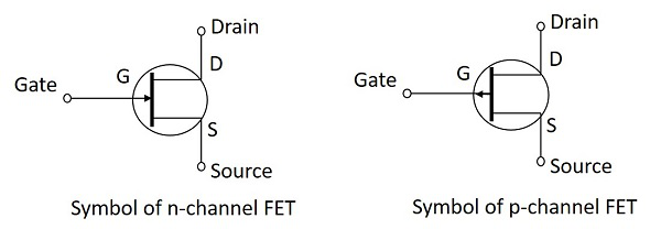
Source
The Source terminal in a Field Effect Transistor is the one through which the carriers enter the channel.
This is analogous to the emitter terminal in a Bipolar Junction Transistor.
The Source terminal can be designated as S.
The current entering the channel at Source terminal is indicated as IS.
Gate
The Gate terminal in a Field Effect Transistor plays a key role in the function of FET by controlling the current through the channel.
By applying an external voltage at Gate terminal, the current through it can be controlled.
Gate is a combination of two terminals connected internally that are heavily doped.
The channel conductivity is said to be modulated by the Gate terminal.
This is analogous to the base terminal in a Bipolar Junction Transistor.
The Gate terminal can be designated as G.
The current entering the channel at Gate terminal is indicated as IG.
Drain
The Drain terminal in a Field Effect Transistor is the one through which the carriers leave the channel.
This is analogous to the collector terminal in a Bipolar Junction Transistor.
The Drain to Source voltage is designated as VDS.
The Drain terminal can be designated as D.
The current leaving the channel at Drain terminal is indicated as ID.
Types of FET
There are two main types of FETS. They are JFET and MOSFET. The following figure gives further classification of FETs.
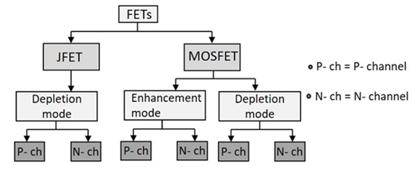
In the subsequent chapters, we will have a detailed discussion on JFET and MOSFET.
Basic Electronics - JFET
The JFET is abbreviated as Junction Field Effect Transistor. JFET is just like a normal FET. The types of JFET are n-channel FET and P-channel FET. A p-type material is added to the n-type substrate in n-channel FET, whereas an n-type material is added to the ptype substrate in p-channel FET. Hence it is enough to discuss one type of FET to understand both.
N-Channel FET
The N-channel FET is the mostly used Field Effect Transistor. For the fabrication of Nchannel FET, a narrow bar of N-type semiconductor is taken on which P-type material is formed by diffusion on the opposite sides. These two sides are joined to draw a single connection for gate terminal. This can be understood from the following figure.
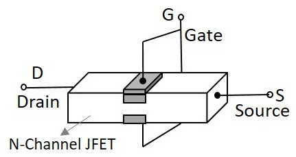
These two gate depositions (p-type materials) form two PN diodes. The area between gates is called as a channel. The majority carriers pass through this channel. Hence the cross sectional form of the FET is understood as the following figure.
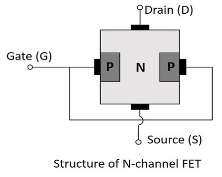
Ohmic contacts are made at the two ends of the n-type semiconductor bar, which form the source and the drain. The source and the drain terminals may be interchanged.
Operation of N-channel FET
Before going into the operation of the FET one should understand how the depletion layers are formed. For this, let us suppose that the voltage at gate terminal say VGG is reverse biased while the voltage at drain terminal say VDD is not applied. Let this be the case 1.
In case 1, When VGG is reverse biased and VDD is not applied, the depletion regions between P and N layers tend to expand. This happens as the negative voltage applied, attracts the holes from the p-type layer towards the gate terminal.
In case 2, When VDD is applied (positive terminal to drain and negative terminal to source) and VGG is not applied, the electrons flow from source to drain which constitute the drain current ID.
Let us now consider the following figure, to understand what happens when both the supplies are given.
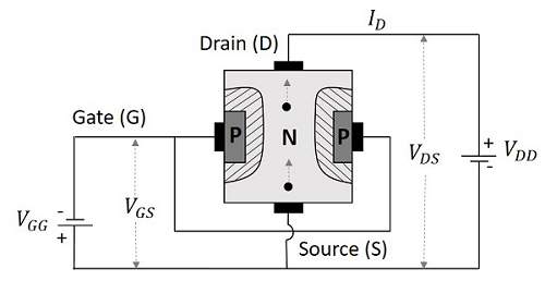
The supply at gate terminal makes the depletion layer grow and the voltage at drain terminal allows the drain current from source to drain terminal. Suppose the point at source terminal is B and the point at drain terminal is A, then the resistance of the channel will be such that the voltage drop at the terminal A is greater than the voltage drop at the terminal B. Which means,
VA>VB
Hence the voltage drop is being progressive through the length of the channel. So, the reverse biasing effect is stronger at drain terminal than at the source terminal. This is why the depletion layer tends to penetrate more into the channel at point A than at point B, when both VGG and VDD are applied. The following figure explains this.
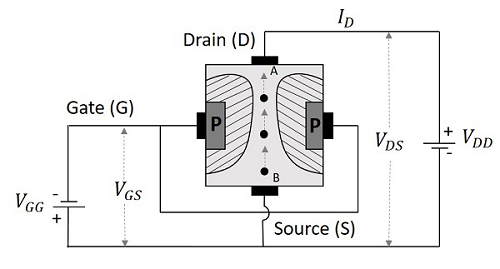
Now that we have understood the behavior of FET, let us go through the real operation of FET.
Depletion Mode of Operation
As the width of depletion layer plays an important role in the operation of FET, the name depletion mode of operation implies. We have another mode called enhancement mode of operation, which will be discussed in the operation of MOSFETs. But JFETs have only depletion mode of operation.
Let us consider that there is no potential applied between gate and source terminals and a potential VDD is applied between drain and source. Now, a current ID flows from drain to source terminal, at its maximum as the channel width is more. Let the voltage applied between gate and source terminal VGG is reverse biased. This increases the depletion width, as discussed above. As the layers grow, the cross-section of the channel decreases and hence the drain current ID also decreases.
When this drain current is further increased, a stage occurs where both the depletion layers touch each other, and prevent the current ID flow. This is clearly shown in the following figure.
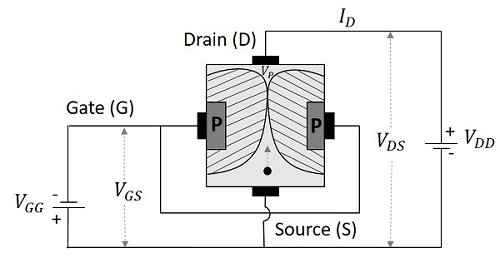
The voltage at which both these depletion layers literally touch is called as Pinch off voltage. It is indicated as VP. The drain current is literally nil at this point. Hence the drain current is a function of reverse bias voltage at gate.
Since gate voltage controls the drain current, FET is called as the voltage controlled device. This is more clearly understood from the drain characteristics curve.
Drain Characteristics of JFET
Let us try to summarize the function of FET through which we can obtain the characteristic curve for drain of FET. The circuit of FET to obtain these characteristics is given below.
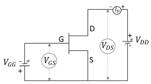
When the voltage between gate and source VGS is zero, or they are shorted, the current ID from source to drain is also nil as there is no VDS applied. As the voltage between drain and source VDS is increased, the current flow ID from source to drain increases. This increase in current is linear up to a certain point A, known as Knee Voltage.
The gate terminals will be under reverse biased condition and as ID increases, the depletion regions tend to constrict. This constriction is unequal in length making these regions come closer at drain and farther at drain, which leads to pinch off voltage. The pinch off voltage is defined as the minimum drain to source voltage where the drain current approaches a constant value (saturation value). The point at which this pinch off voltage occurs is called as Pinch off point, denoted as B.
As VDS is further increased, the channel resistance also increases in such a way that ID practically remains constant. The region BC is known as saturation region or amplifier region. All these along with the points A, B and C are plotted in the graph below.
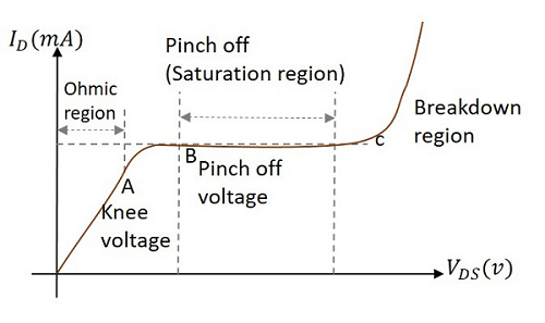
The drain characteristics are plotted for drain current ID against drain source voltage VDS for different values of gate source voltage VGS. The overall drain characteristics for such various input voltages is as given under.
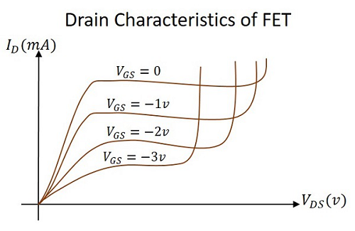
As the negative gate voltage controls the drain current, FET is called as a Voltage controlled device. The drain characteristics indicate the performance of a FET. The drain characteristics plotted above are used to obtain the values of Drain resistance, Transconductance and Amplification Factor.
Basic Electronics - MOSFET
FETs have a few disadvantages like high drain resistance, moderate input impedance and slower operation. To overcome these disadvantages, the MOSFET which is an advanced FET is invented.
MOSFET stands for Metal Oxide Silicon Field Effect Transistor or Metal Oxide Semiconductor Field Effect Transistor. This is also called as IGFET meaning Insulated Gate Field Effect Transistor. The FET is operated in both depletion and enhancement modes of operation. The following figure shows how a practical MOSFET looks like.
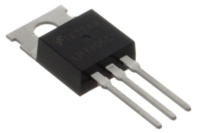
Construction of a MOSFET
The construction of a MOSFET is a bit similar to the FET. An oxide layer is deposited on the substrate to which the gate terminal is connected. This oxide layer acts as an insulator (sio2 insulates from the substrate), and hence the MOSFET has another name as IGFET. In the construction of MOSFET, a lightly doped substrate, is diffused with a heavily doped region. Depending upon the substrate used, they are called as P-type and N-type MOSFETs.
The following figure shows the construction of a MOSFET.
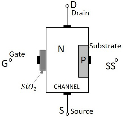
The voltage at gate controls the operation of the MOSFET. In this case, both positive and negative voltages can be applied on the gate as it is insulated from the channel. With negative gate bias voltage, it acts as depletion MOSFET while with positive gate bias voltage it acts as an Enhancement MOSFET.
Classification of MOSFETs
Depending upon the type of materials used in the construction, and the type of operation, the MOSFETs are classified as in the following figure.
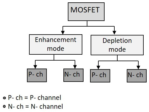
After the classification, let us go through the symbols of MOSFET.
The N-channel MOSFETs are simply called as NMOS. The symbols for N-channel MOSFET are as given below.
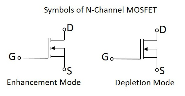
The P-channel MOSFETs are simply called as PMOS. The symbols for P-channel MOSFET are as given below.
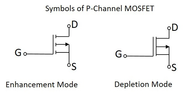
Now, let us go through the constructional details of an N-channel MOSFET. Usually an NChannel MOSFET is considered for explanation as this one is mostly used. Also, there is no need to mention that the study of one type explains the other too.
Construction of N- Channel MOSFET
Let us consider an N-channel MOSFET to understand its working. A lightly doped P-type substrate is taken into which two heavily doped N-type regions are diffused, which act as source and drain. Between these two N+ regions, there occurs diffusion to form an Nchannel, connecting drain and source.
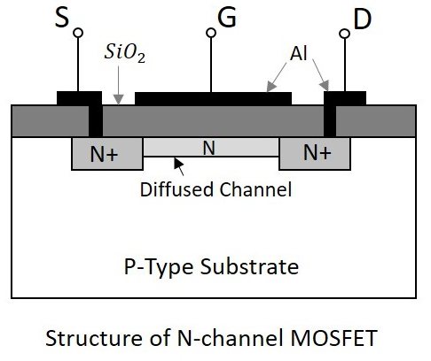
A thin layer of Silicon dioxide (SiO2) is grown over the entire surface and holes are made to draw ohmic contacts for drain and source terminals. A conducting layer of aluminum is laid over the entire channel, upon this SiO2 layer from source to drain which constitutes the gate. The SiO2 substrate is connected to the common or ground terminals.
Because of its construction, the MOSFET has a very less chip area than BJT, which is 5% of the occupancy when compared to bipolar junction transistor. This device can be operated in modes. They are depletion and enhancement modes. Let us try to get into the details.
Working of N - Channel (depletion mode) MOSFET
For now, we have an idea that there is no PN junction present between gate and channel in this, unlike a FET. We can also observe that, the diffused channel N (between two N+ regions), the insulating dielectric SiO2 and the aluminum metal layer of the gate together form a parallel plate capacitor.
If the NMOS has to be worked in depletion mode, the gate terminal should be at negative potential while drain is at positive potential, as shown in the following figure.
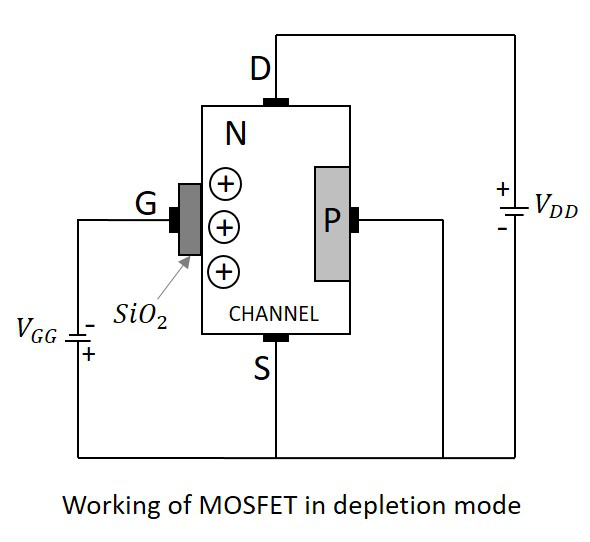
When no voltage is applied between gate and source, some current flows due to the voltage between drain and source. Let some negative voltage is applied at VGG. Then the minority carriers i.e. holes, get attracted and settle near SiO2 layer. But the majority carriers, i.e., electrons get repelled.
With some amount of negative potential at VGG a certain amount of drain current ID flows through source to drain. When this negative potential is further increased, the electrons get depleted and the current ID decreases. Hence the more negative the applied VGG, the lesser the value of drain current ID will be.
The channel nearer to drain gets more depleted than at source (like in FET) and the current flow decreases due to this effect. Hence it is called as depletion mode MOSFET.
Working of N-Channel MOSFET (Enhancement Mode)
The same MOSFET can be worked in enhancement mode, if we can change the polarities of the voltage VGG. So, let us consider the MOSFET with gate source voltage VGG being positive as shown in the following figure.
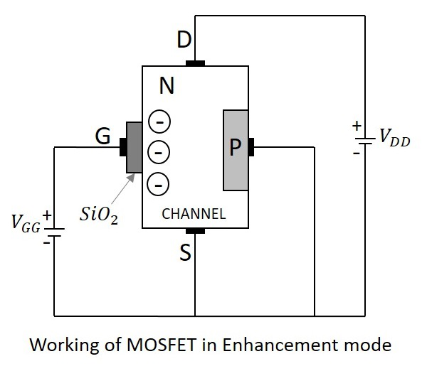
When no voltage is applied between gate and source, some current flows due to the voltage between drain and source. Let some positive voltage is applied at VGG. Then the minority carriers i.e. holes, get repelled and the majority carriers i.e. electrons gets attracted towards the SiO2 layer.
With some amount of positive potential at VGG a certain amount of drain current ID flows through source to drain. When this positive potential is further increased, the current ID increases due to the flow of electrons from source and these are pushed further due to the voltage applied at VGG. Hence the more positive the applied VGG, the more the value of drain current ID will be. The current flow gets enhanced due to the increase in electron flow better than in depletion mode. Hence this mode is termed as Enhanced Mode MOSFET.
P - Channel MOSFET
The construction and working of a PMOS is same as NMOS. A lightly doped n-substrate is taken into which two heavily doped P+ regions are diffused. These two P+ regions act as source and drain. A thin layer of SiO2 is grown over the surface. Holes are cut through this layer to make contacts with P+ regions, as shown in the following figure.
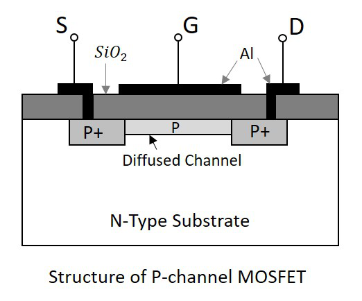
Working of PMOS
When the gate terminal is given a negative potential at VGG than the drain source voltage VDD, then due to the P+ regions present, the hole current is increased through the diffused P channel and the PMOS works in Enhancement Mode.
When the gate terminal is given a positive potential at VGG than the drain source voltage VDD, then due to the repulsion, the depletion occurs due to which the flow of current reduces. Thus PMOS works in Depletion Mode. Though the construction differs, the working is similar in both the type of MOSFETs. Hence with the change in voltage polarity both of the types can be used in both the modes.
This can be better understood by having an idea on the drain characteristics curve.
Drain Characteristics
The drain characteristics of a MOSFET are drawn between the drain current ID and the drain source voltage VDS. The characteristic curve is as shown below for different values of inputs.
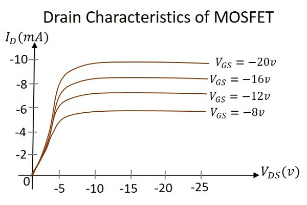
Actually when VDS is increased, the drain current ID should increase, but due to the applied VGS, the drain current is controlled at certain level. Hence the gate current controls the output drain current.
Transfer Characteristics
Transfer characteristics define the change in the value of VDS with the change in ID and VGS in both depletion and enhancement modes. The below transfer characteristic curve is drawn for drain current versus gate to source voltage.
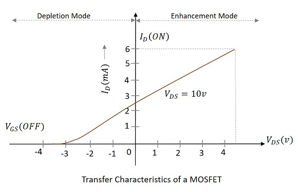
Comparison between BJT, FET and MOSFET
Now that we have discussed all the above three, let us try to compare some of their properties.
| TERMS | BJT | FET | MOSFET |
|---|---|---|---|
| Device type | Current controlled | Voltage controlled | Voltage Controlled |
| Current flow | Bipolar | Unipolar | Unipolar |
| Terminals | Not interchangeable | Interchangeable | Interchangeable |
| Operational modes | No modes | Depletion mode only | Both Enhancement and Depletion modes |
| Input impedance | Low | High | Very high |
| Output resistance | Moderate | Moderate | Low |
| Operational speed | Low | Moderate | High |
| Noise | High | Low | Low |
| Thermal stability | Low | Better | High |
So far, we have discussed various electronic components and their types along with their construction and working. All of these components have various uses in the electronics field. To have a practical knowledge on how these components are used in practical circuits, please refer to the ELECTRONIC CIRCUITS tutorial.
