- Basic Electronics - Materials
- Basic Electronics - Energy Bands
- Basic Electronics - Semiconductors
- Basic Electronics - Hall Effect
- Resistors
- Basic Electronics - Resistors
- Circuit Connections in Resistors
- Non-linear Resistors
- Basic Electronics - Linear Resistors
- Basic Electronics - Fixed Resistors
- Capacitors
- Basic Electronics - Capacitors
- Circuit Connections in Capacitors
- Variable Capacitors
- Basic Electronics - Fixed Capacitors
- Polarized Capacitors
- Inductors
- Basic Electronics - Inductors
- Basic Electronics - Inductance
- Circuit Connections in Inductors
- Types of Inductors
- Basic Electronics - RF Inductors
- Transformers
- Basic Electronics - Transformers
- Types of Transformers
- Transformers based on Usage
- Transformer Efficiency
- Diodes
- Basic Electronics - Diodes
- Basic Electronics - Junction Diodes
- Special Purpose Diodes
- Optoelectronic Diodes
- Transistors
- Basic Electronics - Transistors
- Transistor Configurations
- Transistor Regions of Operation
- Transistor Load Line Analysis
- Types of Transistors
- Basic Electronics - JFET
- Basic Electronics - MOSFET
- Basic Electronics Useful Resources
- Basic Electronics - Quick Guide
- Basic Electronics - Useful Resources
- Basic Electronics - Discussion
Basic Electronics - Semiconductors
A semiconductor is a substance whose resistivity lies between the conductors and insulators. The property of resistivity is not the only one that decides a material as a semiconductor, but it has few properties as follows.
Semiconductors have the resistivity which is less than insulators and more than conductors.
Semiconductors have negative temperature co-efficient. The resistance in semiconductors, increases with the decrease in temperature and vice versa.
The Conducting properties of a Semiconductor changes, when a suitable metallic impurity is added to it, which is a very important property.
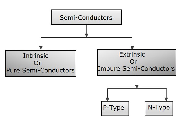
Semiconductor devices are extensively used in the field of electronics. The transistor has replaced the bulky vacuum tubes, from which the size and cost of the devices got decreased and this revolution has kept on increasing its pace leading to the new inventions like integrated electronics. The following illustration shows the classification of semiconductors.
Conduction in Semiconductors
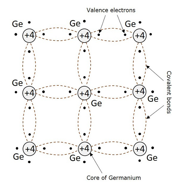
After having some knowledge on the electrons, we came to know that the outermost shell has the valence electrons which are loosely attached to the nucleus. Such an atom, having valence electrons when brought close to the other atom, the valence electrons of both these atoms combine to form Electron pairs. This bonding is not so very strong and hence it is a Covalent bond.
For example, a germanium atom has 32 electrons. 2 electrons in first orbit, 8 in second orbit, 18 in third orbit, while 4 in last orbit. These 4 electrons are valence electrons of germanium atom. These electrons tend to combine with valence electrons of adjoining atoms, to form the electron pairs, as shown in the following figure.
Creation of Hole
Due to the thermal energy supplied to the crystal, some electrons tend to move out of their place and break the covalent bonds. These broken covalent bonds, result in free electrons which wander randomly. But the moved away electrons creates an empty space or valence behind, which is called as a hole.
This hole which represents a missing electron can be considered as a unit positive charge while the electron is considered as a unit negative charge. The liberated electrons move randomly but when some external electric field is applied, these electrons move in opposite direction to the applied field. But the holes created due to absence of electrons, move in the direction of applied field.
Hole Current
It is already understood that when a covalent bond is broken, a hole is created. Actually, there is a strong tendency of semiconductor crystal to form a covalent bond. So, a hole doesnt tend to exist in a crystal. This can be better understood by the following figure, showing a semiconductor crystal lattice.
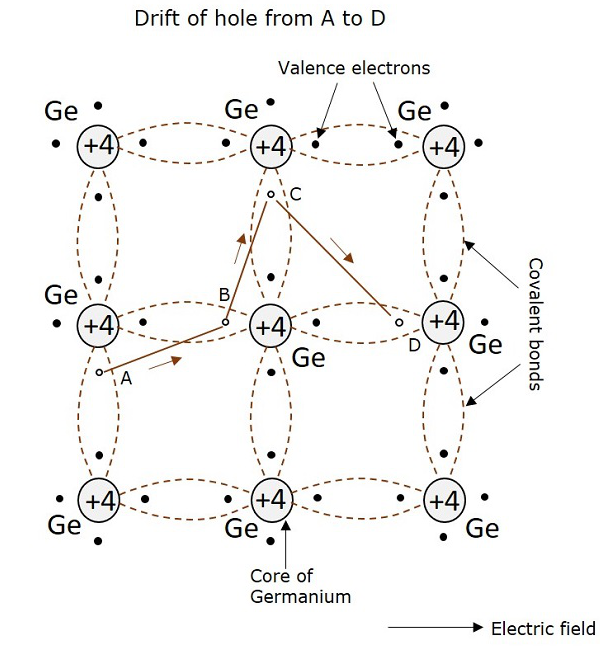
An electron, when gets shifted from a place A, a hole is formed. Due to the tendency for the formation of covalent bond, an electron from B gets shifted to A. Now, again to balance the covalent bond at B, an electron gets shifted from C to B. This continues to build a path. This movement of hole in the absence of an applied field is random. But when electric field is applied, the hole drifts along the applied field, which constitutes the hole current. This is called as hole current but not electron current because, the movement of holes contribute the current flow.
Electrons and holes while in random motion, may encounter with each other, to form pairs. This recombination results in the release of heat, which breaks another covalent bond. When the temperature increases, the rate of generation of electrons and holes increase, thus rate of recombination increases, which results in the increase of densities of electrons and holes. As a result, conductivity of semiconductor increases and resistivity decreases, which means the negative temperature coefficient.
Intrinsic Semiconductors
A Semiconductor in its extremely pure form is said to be an intrinsic semiconductor. The properties of this pure semiconductor are as follows −
- The electrons and holes are solely created by thermal excitation.
- The number of free electrons is equal to the number of holes.
- The conduction capability is small at room temperature.
In order to increase the conduction capability of intrinsic semiconductor, it is better to add some impurities. This process of adding impurities is called as Doping. Now, this doped intrinsic semiconductor is called as an Extrinsic Semiconductor.
Doping
The process of adding impurities to the semiconductor materials is termed as doping. The impurities added, are generally pentavalent and trivalent impurities.
Pentavalent Impurities
The pentavalent impurities are the ones which has five valence electrons in the outer most orbit. Example: Bismuth, Antimony, Arsenic, Phosphorus
The pentavalent atom is called as a donor atom because it donates one electron to the conduction band of pure semiconductor atom.
Trivalent Impurities
The trivalent impurities are the ones which has three valence electrons in the outer most orbit. Example: Gallium, Indium, Aluminum, Boron
The trivalent atom is called as an acceptor atom because it accepts one electron from the semiconductor atom.
Extrinsic Semiconductor
An impure semiconductor, which is formed by doping a pure semiconductor is called as an extrinsic semiconductor. There are two types of extrinsic semiconductors depending upon the type of impurity added. They are N-type extrinsic semiconductor and P-Type extrinsic semiconductor.
N-Type Extrinsic Semiconductor
A small amount of pentavalent impurity is added to a pure semiconductor to result in Ntype extrinsic semiconductor. The added impurity has 5 valence electrons.
For example, if Arsenic atom is added to the germanium atom, four of the valence electrons get attached with the Ge atoms while one electron remains as a free electron. This is as shown in the following figure.
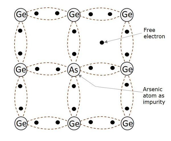
All of these free electrons constitute electron current. Hence, the impurity when added to pure semiconductor, provides electrons for conduction.
In N-type extrinsic semiconductor, as the conduction takes place through electrons, the electrons are majority carriers and the holes are minority carriers.
As there is no addition of positive or negative charges, the electrons are electrically neutral.
When an electric field is applied to an N-type semiconductor, to which a pentavalent impurity is added, the free electrons travel towards positive electrode. This is called as negative or N-type conductivity.
P-Type Extrinsic Semiconductor
A small amount of trivalent impurity is added to a pure semiconductor to result in P-type extrinsic semiconductor. The added impurity has 3 valence electrons. For example, if Boron atom is added to the germanium atom, three of the valence electrons get attached with the Ge atoms, to form three covalent bonds. But, one more electron in germanium remains without forming any bond. As there is no electron in boron remaining to form a covalent bond, the space is treated as a hole. This is as shown in the following figure.
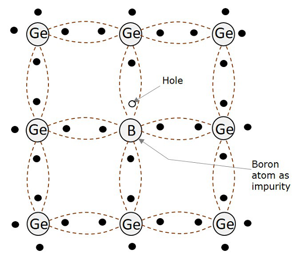
The boron impurity when added in a small amount, provides a number of holes which helps in the conduction. All of these holes constitute hole current.
In P-type extrinsic semiconductor, as the conduction takes place through holes, the holes are majority carriers while the electrons are minority carriers.
The impurity added here provides holes which are called as acceptors, because they accept electrons from the germanium atoms.
As the number of mobile holes remains equal to the number of acceptors, the Ptype semiconductor remains electrically neutral.
When an electric field is applied to a P-type semiconductor, to which a trivalent impurity is added, the holes travel towards negative electrode, but with a slow pace than electrons. This is called as P-type conductivity.
In this P-type conductivity, the valence electrons move from one covalent bond to another, unlike N-type.
Why Silicon is Preferred in Semiconductors?
Among the semiconductor materials like germanium and silicon, the extensively used material for manufacturing various electronic components is Silicon (Si). Silicon is preferred over germanium for many reasons such as −
The energy band gap is 0.7ev, whereas it is 0.2ev for germanium.
The thermal pair generation is smaller.
The formation of SiO2 layer is easy for silicon, which helps in the manufacture of many components along with integration technology.
Si is easily found in nature than Ge.
Noise is less in components made up of Si than in Ge.
Hence, Silicon is used in the manufacture of many electronic components, which are used to make different circuits for various purposes. These components have individual properties and particular uses.
The main electronic components include Resistors, variable resistors, Capacitors, variable capacitors, Inductors, diodes, Tunnel diodes, Varactor diodes, Transistors, BJTs, UJTs, FETs, MOSFETs, LDR, LED, Solar cells, Thermistor, Varistor, Transformer, switches, relays, etc.
