- Basic Electronics - Materials
- Basic Electronics - Energy Bands
- Basic Electronics - Semiconductors
- Basic Electronics - Hall Effect
- Resistors
- Basic Electronics - Resistors
- Circuit Connections in Resistors
- Non-linear Resistors
- Basic Electronics - Linear Resistors
- Basic Electronics - Fixed Resistors
- Capacitors
- Basic Electronics - Capacitors
- Circuit Connections in Capacitors
- Variable Capacitors
- Basic Electronics - Fixed Capacitors
- Polarized Capacitors
- Inductors
- Basic Electronics - Inductors
- Basic Electronics - Inductance
- Circuit Connections in Inductors
- Types of Inductors
- Basic Electronics - RF Inductors
- Transformers
- Basic Electronics - Transformers
- Types of Transformers
- Transformers based on Usage
- Transformer Efficiency
- Diodes
- Basic Electronics - Diodes
- Basic Electronics - Junction Diodes
- Special Purpose Diodes
- Optoelectronic Diodes
- Transistors
- Basic Electronics - Transistors
- Transistor Configurations
- Transistor Regions of Operation
- Transistor Load Line Analysis
- Types of Transistors
- Basic Electronics - JFET
- Basic Electronics - MOSFET
- Basic Electronics Useful Resources
- Basic Electronics - Quick Guide
- Basic Electronics - Useful Resources
- Basic Electronics - Discussion
Basic Electronics - Special Purpose Diodes
There are few diodes which are designed to serve some special purposes. There are many of such kinds like Transient voltage suppression diodes, Gold doped diodes, Super barrier diodes, Point contact diodes, Peltier diodes etc. But other than these, there are few prominent diodes, which have got many applications. Let us go through them.
Varactor Diode
A junction diode has two potentials on both sides where the depletion region can act as a dielectric. Hence there exists a capacitance. The Varactor diode is a special case diode that is operated in reverse bias, where the junction capacitance is varied.
The Varactor diode is also called as Vari Cap or Volt Cap. The following figure shows a Varactor diode connected in reverse bias.
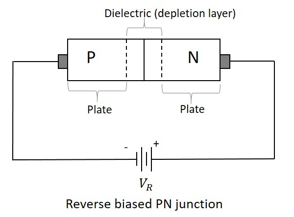
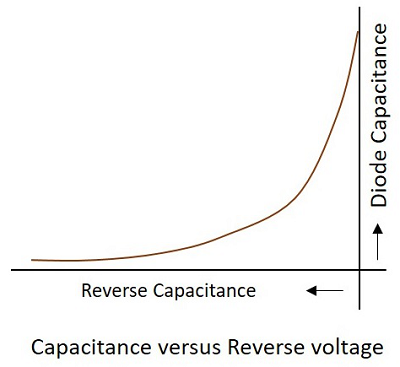
If the reverse voltage applied is increased, the width of the dielectric region increases, which reduces the junction capacitance. When the reverse voltage decreases, the width of the dielectric decreases, which increases the capacitance. If this reverse voltage is completely null, then the capacitance will be at its maximum.
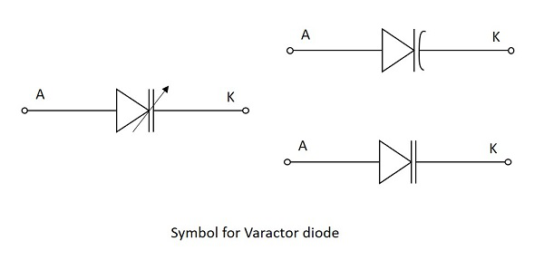
The following figure shows various symbols used for Varactor diode which represents its function.
Though all diodes have this junction capacitance, the Varactor diode is mainly manufactured to make use of this effect and increase the variations in this junction capacitance.
Applications of Varactor diode
This diode has many applications such as −
- It is used as a Voltage variable capacitor.
- It is used in variable LC tank circuit.
- Used as Automatic frequency control.
- Used as Frequency Modulator.
- Used as RF Phase shifter.
- Used as frequency multiplier in local oscillator circuits.
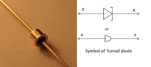
Tunnel diode
If the impurity concentration of a normal PN junction is highly increased, this Tunnel diode is formed. It is also known as Esaki diode, after its inventor.
When the impurity concentration in a diode increases, the width of depletion region decreases, extending some extra force to the charge carriers to cross the junction. When this concentration is further increased, due to less width of the depletion region and the increased energy of the charge carriers, they penetrate through the potential barrier, instead of climbing over it. This penetration can be understood as Tunneling and hence the name, Tunnel diode.
The Tunnel diodes are low power devices and should be handled with care as they easily get affected by heat and static electricity. The Tunnel diode has specific V-I characteristics which explain their working. Let us have a look at the graph below.
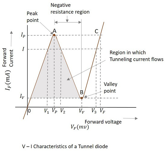
Consider the diode is in forward-biased condition. As forward voltage increases, the current increases rapidly and it increases until a peak point, called as Peak Current, denoted by IP. The voltage at this point is called as Peak Voltage, denoted by VP. This point is indicated by A in the above graph.
If the voltage is further increased beyond VP, then the current starts decreasing. It decreases until a point, called as Valley Current, denoted by IV. The voltage at this point is called as Valley Voltage, denoted by VV. This point is indicated by B in the above graph.
If the voltage is increased further, the current increases as in a normal diode. For larger values of forward voltage, the current increases further beyond.
If we consider the diode is in reverse-biased condition, then the diode acts as an excellent conductor as the reverse voltage increases. The diode here acts as in a negative resistance region.
Applications of Tunnel diode
There are many applications for tunnel diode such as −
- Used as a high-Speed Switching device
- Used as a memory storage device
- Used in Microwave oscillators
- Used in relaxation oscillators
Schottky Diode
This is a special type of diode in which a PN junction is replaced by a metal semiconductor junction. The P-type semiconductor in a normal PN junction diode is replaced by a metal and N-type material is joined to the metal. This combination has no depletion region between them. The following figure shows the Schottky diode and its symbol.
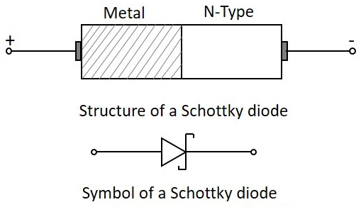
The metal used in this Schottky diode may be gold, silver, platinum or tungsten etc. As well, for the semiconductor material other than silicon, gallium arsenide is mostly used.
Operation
When no voltage is applied or when the circuit is unbiased, the electrons in the N-type material has lower energy level than the ones in the metal. If the diode is then forward biased, these electrons in the N-type gain some energy and move with some higher energy. Hence these electrons are called as Hot Carriers.
The following figure shows a Schottky diode connected in a circuit.
Advantages
There are many advantages of Schottky diode such as −
- It is a unipolar device and hence no reverse currents are formed.
- Its forward resistance is low.
- Voltage drops are very low.
- Rectification is fast and easy with the Schottky diode.
- There is no depletion region present and hence, no junction capacitance. So, the diode gets to OFF position quickly.
Applications
There are many applications of Schottky diode such as −
- Used as a detector diode
- Used as a Power rectifier
- Used in RF mixer circuits
- Used in power circuits
- Used as clamping diodes
