- Basic Electronics - Materials
- Basic Electronics - Energy Bands
- Basic Electronics - Semiconductors
- Basic Electronics - Hall Effect
- Resistors
- Basic Electronics - Resistors
- Circuit Connections in Resistors
- Non-linear Resistors
- Basic Electronics - Linear Resistors
- Basic Electronics - Fixed Resistors
- Capacitors
- Basic Electronics - Capacitors
- Circuit Connections in Capacitors
- Variable Capacitors
- Basic Electronics - Fixed Capacitors
- Polarized Capacitors
- Inductors
- Basic Electronics - Inductors
- Basic Electronics - Inductance
- Circuit Connections in Inductors
- Types of Inductors
- Basic Electronics - RF Inductors
- Transformers
- Basic Electronics - Transformers
- Types of Transformers
- Transformers based on Usage
- Transformer Efficiency
- Diodes
- Basic Electronics - Diodes
- Basic Electronics - Junction Diodes
- Special Purpose Diodes
- Optoelectronic Diodes
- Transistors
- Basic Electronics - Transistors
- Transistor Configurations
- Transistor Regions of Operation
- Transistor Load Line Analysis
- Types of Transistors
- Basic Electronics - JFET
- Basic Electronics - MOSFET
- Basic Electronics Useful Resources
- Basic Electronics - Quick Guide
- Basic Electronics - Useful Resources
- Basic Electronics - Discussion
Basic Electronics - MOSFET
FETs have a few disadvantages like high drain resistance, moderate input impedance and slower operation. To overcome these disadvantages, the MOSFET which is an advanced FET is invented.
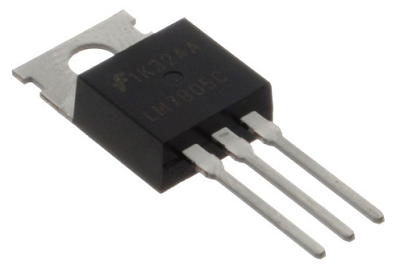
MOSFET stands for Metal Oxide Silicon Field Effect Transistor or Metal Oxide Semiconductor Field Effect Transistor. This is also called as IGFET meaning Insulated Gate Field Effect Transistor. The FET is operated in both depletion and enhancement modes of operation. The following figure shows how a practical MOSFET looks like.
Construction of a MOSFET
The construction of a MOSFET is a bit similar to the FET. An oxide layer is deposited on the substrate to which the gate terminal is connected. This oxide layer acts as an insulator (sio2 insulates from the substrate), and hence the MOSFET has another name as IGFET. In the construction of MOSFET, a lightly doped substrate, is diffused with a heavily doped region. Depending upon the substrate used, they are called as P-type and N-type MOSFETs.
The following figure shows the construction of a MOSFET.
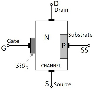
The voltage at gate controls the operation of the MOSFET. In this case, both positive and negative voltages can be applied on the gate as it is insulated from the channel. With negative gate bias voltage, it acts as depletion MOSFET while with positive gate bias voltage it acts as an Enhancement MOSFET.
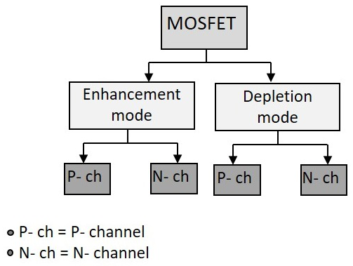
Classification of MOSFETs
Depending upon the type of materials used in the construction, and the type of operation, the MOSFETs are classified as in the following figure.
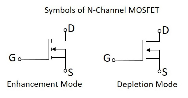
After the classification, let us go through the symbols of MOSFET.
The N-channel MOSFETs are simply called as NMOS. The symbols for N-channel MOSFET are as given below.
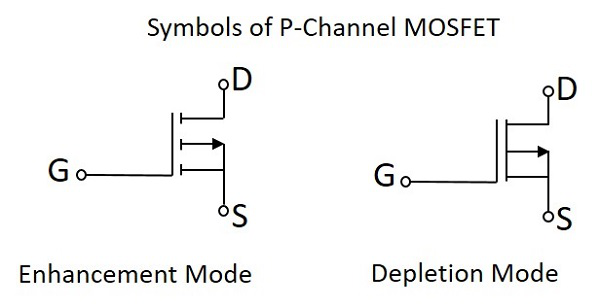
The P-channel MOSFETs are simply called as PMOS. The symbols for P-channel MOSFET are as given below.
Now, let us go through the constructional details of an N-channel MOSFET. Usually an NChannel MOSFET is considered for explanation as this one is mostly used. Also, there is no need to mention that the study of one type explains the other too.
Construction of N- Channel MOSFET
Let us consider an N-channel MOSFET to understand its working. A lightly doped P-type substrate is taken into which two heavily doped N-type regions are diffused, which act as source and drain. Between these two N+ regions, there occurs diffusion to form an Nchannel, connecting drain and source.
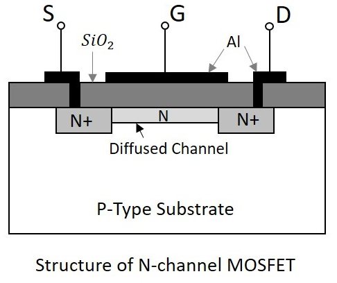
A thin layer of Silicon dioxide (SiO2) is grown over the entire surface and holes are made to draw ohmic contacts for drain and source terminals. A conducting layer of aluminum is laid over the entire channel, upon this SiO2 layer from source to drain which constitutes the gate. The SiO2 substrate is connected to the common or ground terminals.
Because of its construction, the MOSFET has a very less chip area than BJT, which is 5% of the occupancy when compared to bipolar junction transistor. This device can be operated in modes. They are depletion and enhancement modes. Let us try to get into the details.
Working of N - Channel (depletion mode) MOSFET
For now, we have an idea that there is no PN junction present between gate and channel in this, unlike a FET. We can also observe that, the diffused channel N (between two N+ regions), the insulating dielectric SiO2 and the aluminum metal layer of the gate together form a parallel plate capacitor.
If the NMOS has to be worked in depletion mode, the gate terminal should be at negative potential while drain is at positive potential, as shown in the following figure.
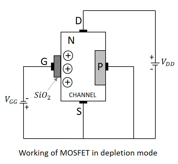
When no voltage is applied between gate and source, some current flows due to the voltage between drain and source. Let some negative voltage is applied at VGG. Then the minority carriers i.e. holes, get attracted and settle near SiO2 layer. But the majority carriers, i.e., electrons get repelled.
With some amount of negative potential at VGG a certain amount of drain current ID flows through source to drain. When this negative potential is further increased, the electrons get depleted and the current ID decreases. Hence the more negative the applied VGG, the lesser the value of drain current ID will be.
The channel nearer to drain gets more depleted than at source (like in FET) and the current flow decreases due to this effect. Hence it is called as depletion mode MOSFET.
Working of N-Channel MOSFET (Enhancement Mode)
The same MOSFET can be worked in enhancement mode, if we can change the polarities of the voltage VGG. So, let us consider the MOSFET with gate source voltage VGG being positive as shown in the following figure.
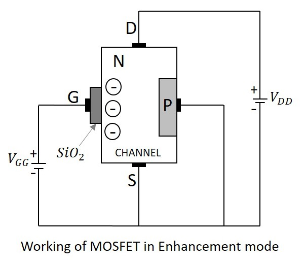
When no voltage is applied between gate and source, some current flows due to the voltage between drain and source. Let some positive voltage is applied at VGG. Then the minority carriers i.e. holes, get repelled and the majority carriers i.e. electrons gets attracted towards the SiO2 layer.
With some amount of positive potential at VGG a certain amount of drain current ID flows through source to drain. When this positive potential is further increased, the current ID increases due to the flow of electrons from source and these are pushed further due to the voltage applied at VGG. Hence the more positive the applied VGG, the more the value of drain current ID will be. The current flow gets enhanced due to the increase in electron flow better than in depletion mode. Hence this mode is termed as Enhanced Mode MOSFET.
P - Channel MOSFET
The construction and working of a PMOS is same as NMOS. A lightly doped n-substrate is taken into which two heavily doped P+ regions are diffused. These two P+ regions act as source and drain. A thin layer of SiO2 is grown over the surface. Holes are cut through this layer to make contacts with P+ regions, as shown in the following figure.
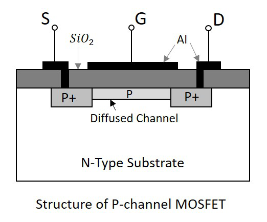
Working of PMOS
When the gate terminal is given a negative potential at VGG than the drain source voltage VDD, then due to the P+ regions present, the hole current is increased through the diffused P channel and the PMOS works in Enhancement Mode.
When the gate terminal is given a positive potential at VGG than the drain source voltage VDD, then due to the repulsion, the depletion occurs due to which the flow of current reduces. Thus PMOS works in Depletion Mode. Though the construction differs, the working is similar in both the type of MOSFETs. Hence with the change in voltage polarity both of the types can be used in both the modes.
This can be better understood by having an idea on the drain characteristics curve.
Drain Characteristics
The drain characteristics of a MOSFET are drawn between the drain current ID and the drain source voltage VDS. The characteristic curve is as shown below for different values of inputs.
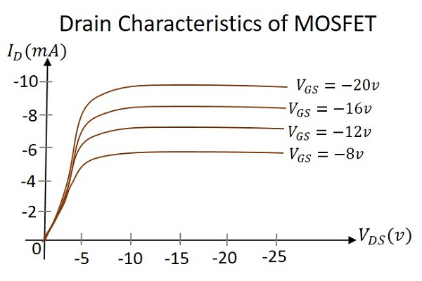
Actually when VDS is increased, the drain current ID should increase, but due to the applied VGS, the drain current is controlled at certain level. Hence the gate current controls the output drain current.
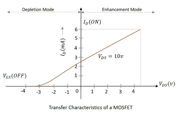
Transfer Characteristics
Transfer characteristics define the change in the value of VDS with the change in ID and VGS in both depletion and enhancement modes. The below transfer characteristic curve is drawn for drain current versus gate to source voltage.
Comparison between BJT, FET and MOSFET
Now that we have discussed all the above three, let us try to compare some of their properties.
| TERMS | BJT | FET | MOSFET |
|---|---|---|---|
| Device type | Current controlled | Voltage controlled | Voltage Controlled |
| Current flow | Bipolar | Unipolar | Unipolar |
| Terminals | Not interchangeable | Interchangeable | Interchangeable |
| Operational modes | No modes | Depletion mode only | Both Enhancement and Depletion modes |
| Input impedance | Low | High | Very high |
| Output resistance | Moderate | Moderate | Low |
| Operational speed | Low | Moderate | High |
| Noise | High | Low | Low |
| Thermal stability | Low | Better | High |
So far, we have discussed various electronic components and their types along with their construction and working. All of these components have various uses in the electronics field. To have a practical knowledge on how these components are used in practical circuits, please refer to the ELECTRONIC CIRCUITS tutorial.
