- Power Electronics - Home
- Power Electronics - Introduction
- Power Electronics - Switching Devices
- Linear Circuit Elements
- Power Electronics - Resistor
- Power Electronics - Inductor
- Power Electronics - Power Diode
- Power Diode - Reverse Recovery Characteristics
- Power Electronics - BJT
- Power Electronics - IGBT
- Power Electronics - MOSFET
- Silicon Controlled Rectifier
- SCR - Switching Characteristics
- Power Electronics - TRIAC
- Power Electronics - GTO Thyristor
- Comparision of Power Semiconductor Devices
- Thyristor - Diode Model
- Thyristor - Two Transistor Model
- Thyristor - Turn ON Methods
- Thyristor - Specifications and Ratings
- Solved Example
- Phase Controlled Converters
- Power Electronics - Pulse Converters
- Effect of Source Inductance
- Performance Parameters
- Reactive Power Control of Converters
- Power Electronics - Dual Converters
- Solved Example
- DC to DC Converters
- Power Electronics - Choppers
- Power Electronics - Control Methods
- Resonant Switching
- DC Converters Solved Example
- AC to DC Converters
- Single Phase AC Voltage Controllers
- Power Electronics - Cycloconverters
- Integral Cycle Control
- Power Electronics - Matrix Converters
- Solved Example
- Power Electronics Resources
- Power Electronics - Quick Guide
- Power Electronics - Useful Resources
- Power Electronics - Discussion
Two Transistor Model Of a Thyristor
The principle of thyristor operation can be explained with the use of its two-transistor model(or two-transistor analogy). It is obtained by bisecting the two middle layers, along the dotted line, in two separate halves as shown in the following figure −
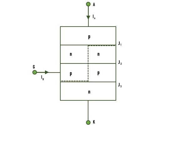
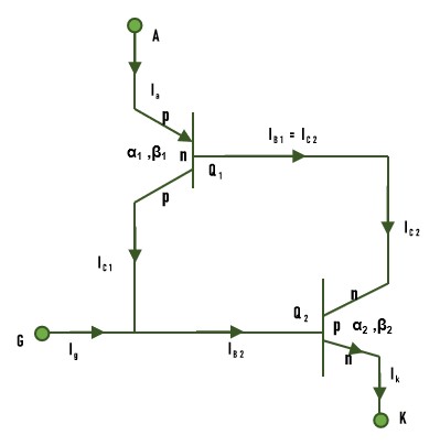
The junction J1 and J2 can be considered as pnp transistor and the junction J2 and J3 can be considered as a npn transistor. The circuit representation of the two transistor model of thyristor is shown in the following −
In the off-state of a transistor, collector current IC is related to emitter current IE can be expressed as −
$$\mathrm{I_C\:=\:\alpha I_E\:+\:I_{CBO}}$$
where α is the common base current gain and ICBO is the common-base leakage current of collector-base junction of a transistor.
For transistor Q1, emitter current IE = anode current Ia and IC = collector current IC1. Therefore , for Q1, −
$$\mathrm{I_{C1}\:=\:\alpha_{1} I_a\:+\:I_{CBO1}\:\:\:\:\:....Eq\:-\:1}$$
$$\mathrm{where\:,\alpha_1\:=\:common-base\:current\:gain\:of\:Q_1} \\ \mathrm{I_{CBO1}\:=\:common-base\:leakage\:current\:of\:Q_1} $$
Similarly, for transistor Q2, the collector current IC2 can be expressed as −
$$\mathrm{I_{C2}\:=\:\alpha_{2} I_k\:+\:I_{CBO2}\:\:\:\:\:....Eq\:-\:2}$$
$\mathrm{where\:,\alpha_2\:=\:common-base\:current\:gain\:of\:Q_2} \\ \mathrm{I_{CBO2}\:=\:common-base\:leakage\:current\:of\:Q_2} \\ \mathrm{I_k\:=\:emitter\:current\:of\:Q_2} $
By applying the KCL at anode terminal we get −
$$\mathrm{I_a\:=\:I_{C1}\:+\:I_{C2}\:\:\:\:\:....Eq\:-\:3}$$
Substituting Eq - 1 and Eq - 2 in the Eq - 3, then anode current Ia can be expressed as −
$$\mathrm{I_a\:=\:\alpha_1 I_a\:+\:I_{CBO1}\:+\:\:\alpha_2 I_k\:+\:I_{CBO2}\:\:\:\:\:....Eq\:-\:4}$$
When gate current is applied, then Ik = Ia + Ig. Substituting this value of Ik in the Eq - 4
$$\mathrm{I_a\:=\:\alpha_1 I_a\:+\:I_{CBO1}\:+\:\:\alpha_2 (I_a+I_g)\:+\:I_{CBO2}}$$
$$\mathrm{I_a\:=\:\alpha_1 I_a\:+\:I_{CBO1}\:+\:\alpha_2 (I_a+I_g)\:+\:I_{CBO2}} \\ \mathrm{\Rightarrow\:Ia\:=\:\alpha_1 I_a\:+\:I_{CBO1}\:+\alpha_2I_a\:+\alpha_2I_g\:+\:I_{CBO2}} \\ \mathrm{\Rightarrow\:I_a\:=\:(\alpha_1\:+\alpha_2)I_a\:+\:\alpha_2I_g\:+\:I_{CBO1}\:+\:I_{CBO2}} \\ \mathrm{\Rightarrow\:I_a[1-(\alpha_1\:+\alpha_2)]\:=\:\alpha_2I_g\:+\:I_{CBO1}\:+\:I_{CBO2}} \\ \mathrm{\therefore\:I_a\:=\:\frac{\alpha_2I_g\:+\:I_{CBO1}\:+\:I_{CBO2}}{1-(\alpha_1\:+\alpha_2)} } $$
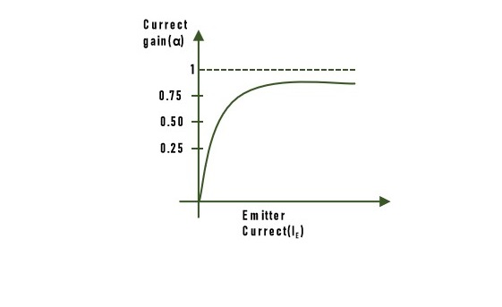
Current gain α is very low at low emitter current. With an increase in emitter current. With an increase in emitter current, α increases rapidly as shown in the graph below −
If, by some means, the emitter current of two transistors Q1 and Q2 is increased so that $\mathrm{\alpha_1\:+\:\alpha_2}$ approaches unity, then as per equation, Ia would tend to become infinite, which implies that the device has turned ON.
Therefore, the methods of turning on the device are nothing but the methods of making $\mathrm{\alpha_1\:+\:\alpha_2}$ to approach unity, that is $\mathrm{(\alpha_1\:+\:\alpha_2)\:\approxeq\:1}$.
