- Power Electronics - Home
- Power Electronics - Introduction
- Power Electronics - Switching Devices
- Linear Circuit Elements
- Power Electronics - Resistor
- Power Electronics - Inductor
- Power Electronics - Power Diode
- Power Diode - Reverse Recovery Characteristics
- Power Electronics - BJT
- Power Electronics - IGBT
- Power Electronics - MOSFET
- Silicon Controlled Rectifier
- SCR - Switching Characteristics
- Power Electronics - TRIAC
- Power Electronics - GTO Thyristor
- Comparision of Power Semiconductor Devices
- Thyristor - Diode Model
- Thyristor - Two Transistor Model
- Thyristor - Turn ON Methods
- Thyristor - Specifications and Ratings
- Solved Example
- Phase Controlled Converters
- Power Electronics - Pulse Converters
- Effect of Source Inductance
- Performance Parameters
- Reactive Power Control of Converters
- Power Electronics - Dual Converters
- Solved Example
- DC to DC Converters
- Power Electronics - Choppers
- Power Electronics - Control Methods
- Resonant Switching
- DC Converters Solved Example
- AC to DC Converters
- Single Phase AC Voltage Controllers
- Power Electronics - Cycloconverters
- Integral Cycle Control
- Power Electronics - Matrix Converters
- Solved Example
- Power Electronics Resources
- Power Electronics - Quick Guide
- Power Electronics - Useful Resources
- Power Electronics - Discussion
Switching Characteristics of SCR
Static and switching characteristics of SCR(thyristors) are always taken into consideration for economical and reliable design of converter equipment. We have discussed static characteristics in the previous chapter. In this section, we will discuss the switching, dynamic or transient characteristics of SCR.
During turn-on an turn-off processes, a SCR is subjected to different voltages across it and different current through it. The time variations of the voltage across a thyristor and the current through it during turn-on and turn-off processes is given by the dynamic or switching characteristics of a thyristor.
Switching Characteristics during Turn-on
When the thyristor is forward biased and a positive gate pulse is applied between the gate and cathode, it will be turned ON, but there is a finite transition time to switch from forward OFF state to forward ON state for a thyristor. This finite transition time is known as a turn-ON time.
Following conditions must be satisfied to turn-on a thyristor −
- Thyristor must be forward biased and anode potential must be positive with respective to cathode.
- The width of gate pulse must be greater than the turn-on time of thyristor. Anode current must be greater than latching current when the gate signal is removed.
- Anode to cathode voltage must be greater than finger voltage, it is the minimum anode voltage that must be maintained across the SCR, so that it can be triggered by giving any value of gate current.
- Amplitude of gate current must be more than the minimum gate current which is required to turn-on SCR.
- Amplitude of gate current must be less than the maximum permissible gate current so that gate circuit may not be damaged.
- The gate triggering must be synchronized with ac supply.
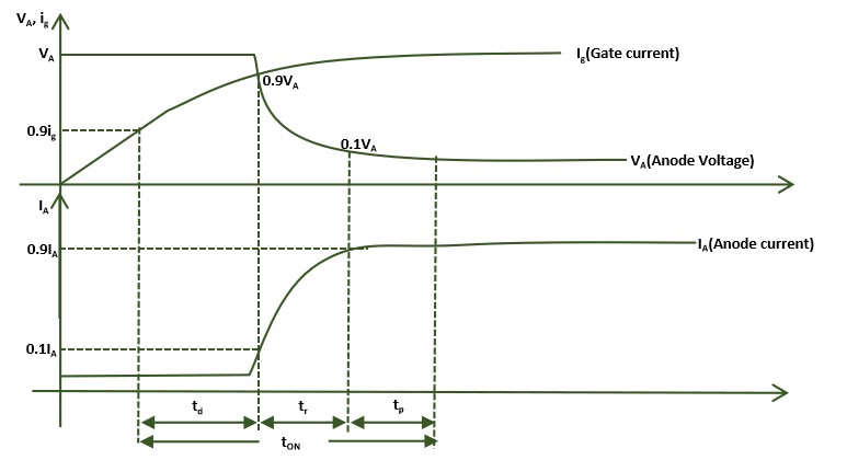
The turn-ON time tturn-ON is the sum of the delay time (td), rise-time (tr) and spread time (tp) and it can be expressed as −
$\mathrm{t_{turn-ON}\:=\:t_d\:+\:t_r\:+\:t_p}$
Delay time (td)
There is a time delay to turn-on a device. The delay time td is the required time interval from initial anode current i.e, forward leakage current to reach 10% of final value of anode current(0.1IA) where IA is the final value of anode current.
The delay time (td) can be measured from the instant of the gate current reaches 0.9Ig to the instant at which anode current reaches to 0.1IA is the final value of anode current.
The delay time td can also be measured by the time interval during which anode voltage falls from VA to 0.9VA where VA is the initial value of anode to cathode voltage
Rise time (tr)
The rise time tr is the time interval during which the cathode current increases from 10% to 90% of final anode current. During rise time the forward blocking OFF state voltage decreases, the rise time tr can be measured from the instant of 90% of forward blocking OFF-state voltage (0.9VA) to the instant at which forward blocking OFF-state voltage reaches to 0.1VA.
The rise time (tr) can also be measured from the instant of the gate current reaches 0.9Ig to the instant at which gate current Ig where Ig is the final value of gate current. The rise time is inversely proportional to the amplitude of the gate current and its build up rate.
Spread time (tp)
The spread time is the time interval during blocking which the forward blocking voltage falls from 10% of its value to the ON-state voltage drop about 1V to 1.5V.
The spread time can be defined as the time taken by the anode current to rise from 0.9IA to IA. During this time, the conduction spreads over the entire cross section of the SCR cathode. The spreading time depends on the area of the cathode and gate structure of SCR.
After spread time tp, SCR is completely turned ON and finally steady state anode current flows through device and the voltage drop across SCR is 1V to 1.5V. The total turn ON time of SCR is equal to 1 to 4ms.
Switching Characteristics during Turn-off
When a thyristor is in conducting state and it can be turned OFF if the anode current is reduced slowly below the holding current IH. The turn-OFF process of the thyristor is called commutation. There are two primary methods for turning OFF a thyristor(SCR) −
- Natural Commutation
- Forced Commutation
Following conditions must be satisfied to turn OFF a thyristor −
- A thyristor(SCR) can be turned OFF when its forward current IA is reduced below the holding current IH.
- When a reverse voltage is applied across the thyristor for a specified time so that the device recover to the blocking state.
- After it is turned OFF, the forward voltage can be re-applied after certain time so that the excess carriers in the outer and inner layers of the SCR have to decay adequately.
- The decay and recombination of excess carriers can be accelerated by applying a reverse voltage across the SCR.
The turn OFF time of a SCR tq can be defined as the time interval between the instant at which anode current through the device becomes zero and the instant at which SCR regain its forward blocking capability.
The turn OFF time of a SCR tq is the sum of the reverse recovery time (trr) and gate recovery time (tgr) and it can be expressed as −
$\mathrm{t_{q}\:=\:t_{rr}\:+\:t_{gr}}$
Reverse Recovery time (trr)
From the characteristics, at time t=t1 the anode current becomes zero. After t=t1, anode current starts to build up in the reverse direction due to presence of charge carriers in the reverse direction due to presence of charge carriers in the four layers of SCR. Actually, the reverse recovery current removes the excess charge carriers from junctions J1 and J3 during the time interval between t=t1 and t=t3.
Consequently, the holes are sweeping out from top p-layer and the electrons are sweeping out from bottom n-layer. At t=t2, about 60% of the stored charge carriers are removed from outer two layers, i.e., top p-layer and bottom n-layer. As a result, the carrier density in junction J1 and J3 decreases and subsequently the reverse recovery current also decreases.
Initially the rate of reverse recovery current is very fast but it is gradually decrease thereafter, due to the fast decay of reverse recovery current, a reverse surge voltage appeared across the SCR and the device may be damaged. This condition may be avoided by using RC snubber circuit across SCR.
Gate Recovery time (tgr)
At the time t=t3, the reverse recovery current becomes very small and its value is about zero and the thyristor is t=t1 and t=t3, all excess charge carriers are removed from outer junctions J1 and J3.
At t=t3, the middle junction J2 still consists of charge carriers and it cannot able to block the forward voltage. Since the charge carriers present in the junction J2 cannot able to flow to the external circuit, these carriers can be removed by recombination only. The recombination is possible when a reverse voltage is applied across SCR for a specific time.
The rate of recombination does not depend on the external circuit parameters. The recombination of charge carriers take place between t=t3 and t=t4. The time interval between t=t1 and t=t3 is called gate recovery time tgr. At t=t4, thyristor operates in OFF state.
