- Power Electronics - Home
- Power Electronics - Introduction
- Power Electronics - Switching Devices
- Linear Circuit Elements
- Power Electronics - Resistor
- Power Electronics - Inductor
- Power Electronics - Power Diode
- Power Diode - Reverse Recovery Characteristics
- Power Electronics - BJT
- Power Electronics - IGBT
- Power Electronics - MOSFET
- Silicon Controlled Rectifier
- SCR - Switching Characteristics
- Power Electronics - TRIAC
- Power Electronics - GTO Thyristor
- Comparision of Power Semiconductor Devices
- Thyristor - Diode Model
- Thyristor - Two Transistor Model
- Thyristor - Turn ON Methods
- Thyristor - Specifications and Ratings
- Solved Example
- Phase Controlled Converters
- Power Electronics - Pulse Converters
- Effect of Source Inductance
- Performance Parameters
- Reactive Power Control of Converters
- Power Electronics - Dual Converters
- Solved Example
- DC to DC Converters
- Power Electronics - Choppers
- Power Electronics - Control Methods
- Resonant Switching
- DC Converters Solved Example
- AC to DC Converters
- Single Phase AC Voltage Controllers
- Power Electronics - Cycloconverters
- Integral Cycle Control
- Power Electronics - Matrix Converters
- Solved Example
- Power Electronics Resources
- Power Electronics - Quick Guide
- Power Electronics - Useful Resources
- Power Electronics - Discussion
Power Electronics - SCR(Thyristor)
The word Thyristor is derived by a combination of the THYRathon and tranSTOR, which means that thyristor is a solid state device like transistor and has a characteristics similar to that of the thyratron tube. SCR is one of the semiconductor device in thyristor family
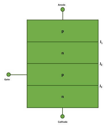
Silicon Controlled Rectifier is a four layers of alternate p-type and n-type semiconductors forming three junctions J1, J2 and J2. The terminal connected to outer p-type is anode, the terminal connected to outer n-type is cathode and the terminal connected to the inner p-type is gate terminal. It is a bipolar blocking device, uni-direction conducting device and pulse triggered switch. It is a semi-controlled switch where we can controlled by the device.
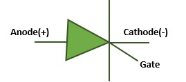
A SCR is so called because silicon is used for its construction and its operation as a rectifier(very low resistance in forward conduction and very high resistance in reverse direction) can be controlled. A SCR blocks the current flow from anode to cathode until it is triggered into conduction by a proper gate signal between gate and cathode terminals.
SCR - Mode of Operations
The SCR operates in three basic modes −
- Reverse Blocking Mode
- Forward Blocking Mode
- Forward Conduction Mode
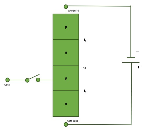
Reverse Blocking Mode
When cathode is made positive with respect to anode with switch (S) open, SCR is reverse biased. Junctions J1, J3 are reversed biased, whereas junction J2 is forward biased. In this mode, the device behaves as if two diodes are connected in series with reverse voltage applied across them.
A small leakage current of the order of a d=few milli-amperes flows. This is reverse blocking mode is also known as OFF-state of SCR. If the reverse voltage is increased, then at a critical breakdown level, called reverse breakdown voltage VBR, an avalanche occurs at J1 and J3 and the reverse breakdown voltage increases rapidly.
A larger current associated with VBR gives rise to more losses, leads to damage of SCR. Therefore, the reverse voltage across the SCR should not exceed the VBR. When reverse applied across the SCR is less than VBR, the device offers a high impedance in reverse direction, therefore SCR in the reverse blocking mode can be treated as an open switch.
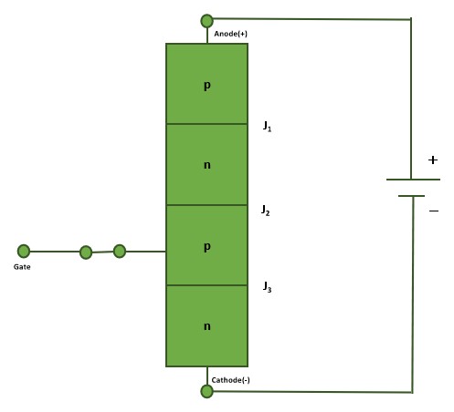
Forward Blocking Mode
When anode is positive with respect to the cathode, with gate circuit open, SCR is said to be forward biased. In this mode junction J1 and J3 are forward biased and junction J2 is reverse biased.
In this mode, a small forward leakage current flows. If the forward voltage is increased, then the reverse biased junction J2 will have an avalanche breakdown at a voltage called forward break-over voltage VBO. When forward voltage is less than VBO, SCR offers a high impedance. Therefore, SCR can be treated as an open switch even in the forward blocking mode.

Forward Conduction Mode
In this mode, SCR conducts current from anode to cathode with a very small voltage drop across it. SCR is brought from forward break-over voltage to forward conduction mode by turning it on by exceeding the forward break-over voltage or by applying a gate pulse between gate and cathode.
In this mode, SCR is in ON- state and behaves like a closed switch. Voltage drop across SCR in the ON state is of the order of 1 to 2V depending on the rating of SCR.
SCR - static VI characteristics
Following are the static V - I characteristics of SCR
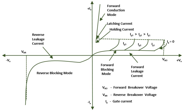
Latching Current(IL)
The minimum value of anode current which it must attain during turn-ON process to maintain conduction when gate signal is removed. It is associated with turn-ON process.
Holding Current(IH)
The minimum value of anode current below which it must fall for turning-OFF the scr. It is associated with turning-OFF process.
The latching current (IL) is taken as two or three times the holding current(IH).
