- Power Electronics - Home
- Power Electronics - Introduction
- Power Electronics - Switching Devices
- Linear Circuit Elements
- Power Electronics - Resistor
- Power Electronics - Inductor
- Power Electronics - Power Diode
- Power Diode - Reverse Recovery Characteristics
- Power Electronics - BJT
- Power Electronics - IGBT
- Power Electronics - MOSFET
- Silicon Controlled Rectifier
- SCR - Switching Characteristics
- Power Electronics - TRIAC
- Power Electronics - GTO Thyristor
- Comparision of Power Semiconductor Devices
- Thyristor - Diode Model
- Thyristor - Two Transistor Model
- Thyristor - Turn ON Methods
- Thyristor - Specifications and Ratings
- Solved Example
- Phase Controlled Converters
- Power Electronics - Pulse Converters
- Effect of Source Inductance
- Performance Parameters
- Reactive Power Control of Converters
- Power Electronics - Dual Converters
- Solved Example
- DC to DC Converters
- Power Electronics - Choppers
- Power Electronics - Control Methods
- Resonant Switching
- DC Converters Solved Example
- AC to DC Converters
- Single Phase AC Voltage Controllers
- Power Electronics - Cycloconverters
- Integral Cycle Control
- Power Electronics - Matrix Converters
- Solved Example
- Power Electronics Resources
- Power Electronics - Quick Guide
- Power Electronics - Useful Resources
- Power Electronics - Discussion
Power Electronics - Power BJT
The Bipolar Junction Transistor (BJT) is a three-layer, two-junction semiconductor device that can be either NPN or PNP in structure. The term bipolar signifies that current flow in the device is due to the movement of both holes and electrons. The term junction refers to the interface formed when P-type and N-type semiconductor materials are joined together. The word transistor is derived from transferred resistor, indicating that a small input current or voltage controls a larger output current or voltage, thereby enabling amplification.
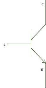
Construction details of Power BJT
BJT has three terminals collector, emitter and base. A emitter is indicated by an down head indicating the directing the direction of emitter current.
Following are the terminals of Power BJT −
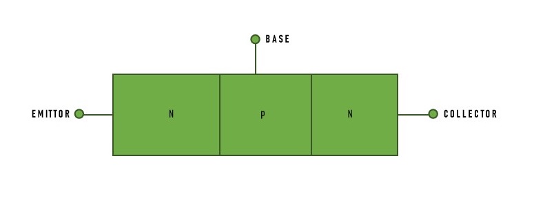
- Emitter: The emitter is heavily doped to ensure a high injection of charge carriers. It is designed with a medium-sized area to provide optimal current flow.
- Collector: The collector is moderately doped and designed with a larger area to handle high power dissipation and collect the majority of carriers.
- Base: The base is lightly doped and has a small area to facilitate efficient control of the emitter-collector current and to reduce recombination losses.
when transistor is in active region, then jc junction is reversed biased. If the collector is heavily doped the breakdown voltage vBr will be very less so collector should be moderately doped.
BJT Modes of Operation
Following are the modes of operation of BJT −
| Mode Of Operation | JE | JC | Property | Application |
|---|---|---|---|---|
| cut-off region | RB | RB | High resistance | OFF switch |
| Saturation region | FB | FB | Low resistance | ON switch |
| Active region | FB | RB | Transistor | Amplifier |
| Reverse active mode or Inverted mode | RB | FB | Reverse transistor action | Attenuation |
Power BJT Configurations
When a transistor is to be connected in a circuit, one terminal is used as an input terminal, the other terminal is used as an output terminal, and the third terminal is common to the input and output. Depending upon the input, output, and common terminals, a transistor can be connected in three configurations. They are −
- Common Base (CB) configuration
- Common Emitter (CE) configuration
- Common Collector (CC) configuration
BJT - Common Base (CB) configuration
This is also called grounded-base configuration. In this configuration, the emitter is the input terminal, the collector is the output terminal, and the base is the common terminal.
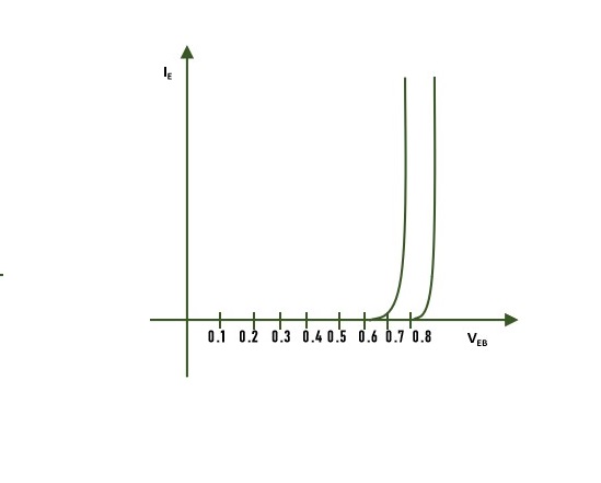
Input Characteristics of Common Base Configuration
To determine the input characteristics, the collector-base voltage VCB is kept constant at zero volt and the emitter current IE is increased from zero in suitable equal steps by increasing VEB. This is repeated for higher fixed values of VCB. A curve is drawn between emitter current IE and emitter-base voltage VEB at constant collector-base voltage VCB. The input characteristics thus obtained are shown in the following figure
Output Characteristics of Common Base Configuration
To determine the output characteristics, the emitter current IE is kept constant at a suitable value by adjusting the emitter-base voltage VEB. Then VCB is increased in suitable equal steps and the collector current IC is noted for each value of IE. This is repeated for different fixed values of IE. Now the curves of IC versus VCB are plotted for constant values of IE and the output characteristics thus obtained
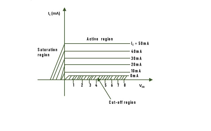
From the characteristics, it is seen that for a constant value of IE, IC is independent of VCB and the curves are parallel to the axis of VCB. Further, IC flows even when VCB is equal to zero. As the emitter-base junction is forward biased, the majority carriers, i.e., electrons, from the emitter are injected into the base region. Due to the action of the internal potential barrier at the reverse-biased collector-base junction, they flow to the collector region and give rise to IC even when VCB is equal to zero.
As the collector voltage VCC is made to increase the reverse bias, the space charge width between collector and base tends to increase, with the result that the effective width of the base decreases. This dependency of base width on collector-to-base voltage is known as the Early effect. This decrease in effective base width has three consequences −
- There is less chance for recombination within the base region. Hence, a increases with increasing |VCB|.
- The charge gradient is increased within the base, and consequently, the current of minority carriers injected across the emitter junction increases.
- For extremely large voltages, the effective base width may be reduced to zero, causing voltage breakdown in the transistor. This phenomenon is called the punch-through.
In the dc mode the levels of IC and IE due to the majority carriers are related by a quantity called alpha and defined by the following equation −
$$\mathrm{ \alpha\:=\: \frac{I_C}{I_E} }$$
BJT in Active Mode
Consider a pnp transistor, emitter junction(JE) is forward biased and collector junction(JC) is reversed biased then the bjt is said to be in active region.
Current in the emitter is due to flow of holes from emitter to base and flow of electrons(e-) from base to emitter −
$$\mathrm{I_E\:=\:I_{pE}\:+\:I_{nE}}$$
where, IpE = holes from emitter to base
InE = electrons from base to emitter
$$\mathrm{N_E\:\gg\:N_{pE}\:\:\:\:(concentration\:of\:emitter\:\ggg\:concentration\:of\:base)}$$
$$\mathrm{\therefore I_E\:\approx\:I_{pE}} $$
Emitter efficiency or Emitter injection efficiency($\mathrm{\gamma}$)
It is the ratio of current due to injected at the emitter-base junction to total emitter current.
$$\mathrm{\gamma\:=\frac{I_{pE}}{I_E}}$$
If the concentration of the emitter greater than concentration of base($\mathrm{N_E\:\gg\:N_{pE}}$) then $\mathrm{\gamma\:\approx\:1} $
As the doping level of base is lesser and holes from the emitter entered the base few will take part in recombination and most of the holes will enter JC junction as there were attracted by the negative terminals and this causes a collector current IpC.
Transport factor($\mathrm{\beta^*}$)
It is the ratio of collector current due to injected carrier reaching base to collector junction to the injected carrier current at emitter-base junction.
$$\mathrm{\beta^*\:=\:\frac{I_{pC}}{I_{pE}}}$$
$$\mathrm{\beta^*\:=\:\frac{Holes\:current\:in\:the\:collector}{Holes\:current\:in\:the\:\:emitter}}$$
the value of $\mathrm{\beta^*}$ is less than or equal to 1 i.e., $\mathrm{\beta^*\:\leq\:1}$
BJT - Current Control Device
If additional electrons (e-) are supplied to the base junction, a larger emitter current(IE) flows, as the increased number of electrons attracts more holes from the emitter. As a result, the emitter current (IE) increases. Since the base current (IB) directly influences the emitter current (IE), and we can control IB, the BJT is referred to as a current-controlled device.
recombination current IB = IpE - IpC
$$\mathrm{\therefore\: total\:current(I_C)\:=\:I_{pC}\:+\:I_{C_0}}$$
$\mathrm{where\:,\:I_{C_0}\:=\:small\:current\:due\:to\:reverse\:bias\: or\:reverse\:saturation\:current}$
Expression of Collector current(IC) in Active mode
Consider pnp transistor, forward biased is applied across JE and reverse biased at collector junction JC, then collector current can be given by −
$$\mathrm{I_C\:=\:I_{pC}\:+\:I_{C_0}\:\:\:\:\:....eq1}$$
by applying kirrchoff laws,
$$\mathrm{I_E\:=\:I_{B}\:+\:I_{C}\:\:\:\:\:....eq2}$$
$$\mathrm{\alpha\:=\:\frac{\Delta I_C}{\Delta I_E}\:=\:\frac{I_{pC}}{I_E}}$$
$$\mathrm{\Rightarrow I_{pC}\:=\:\alpha\:{I_E}\:\:\:\:\:....eq3}$$
substituting eq3 in eq1
$$\mathrm{I_{C}\:=\:\alpha\:{I_E}\:+\:I_{C_0}}$$
$$\mathrm{I_{C}\:=\:\alpha\:[I_{B}\:+\:I_{C}]\:+\:I_{C_0}}$$
$$\mathrm{\Rightarrow I_{C}\:=\:\alpha\:I_{B}\:+\:\alpha I_{C}\:+\:I_{C_0}}$$
$$\mathrm{\Rightarrow I_{C}\:-\:\:\alpha I_{C}\:=\:\alpha\:I_{B}\:+\:I_{C_0}}$$
$$\mathrm{\Rightarrow I_{C}[1\:-\:\alpha]\:=\:\alpha\:I_{B}\:+\:I_{C_0}}$$
$$\mathrm{\Rightarrow I_{C}[1\:-\:\alpha]\:=\:\alpha\:I_{B}\:+\:I_{C_0}} $$
$$\mathrm{\therefore\:I_{C}\:=\: (\frac{\alpha}{1\:-\:\alpha})\:I_{B}\:+\:(\frac{1}{1\:-\:\alpha})I_{C_0}\:\:\:\:\:...eq4}$$
Now replace, $\mathrm{\alpha}$ in terms of $\mathrm{\beta}$
$$\mathrm{\beta\:=\:\frac{\alpha}{1\:-\:\alpha}\:\:\:\:\:and \:\:\:\:\beta\:+\:1=\:\frac{1}{1\:-\:\alpha}\: \:\:\:\:substitute\:in\:eq4}$$
$$\mathrm{I_{C}\:=\:\beta\:I_{B}\:+\:(\beta+1)I_{C_0}}$$
Example : A BJT has $\mathrm{\alpha\:=\:0.99,\:I_{C_0}\:=\:50nA}$ and it is operating at a basic current of $\mathrm{10\mu A}$, calcuate $\mathrm{I_C,\:I_{CB0,}\:I_{CE0}}$?
Solution : Given, α = 0.99, $\mathrm{I_{CO}\:=\:50nA,\:I_B\:=\:10\mu A}$
we know, $\mathrm{I_{C}\:=\:\alpha I_E\:+\:I_{CO}\:\:\:\:\:....eq1}$
$\mathrm{I_{C}\:=\:\beta I_E\:+\:(\beta+1)I_{CO}\:\:\:\:\:....eq2}$
$\mathrm{\beta\:=\:\frac{\alpha}{1\:-\:\alpha}}$
$\mathrm{\Rightarrow \beta\:=\:\frac{0.99}{1\:-\:0.99}}$
$\mathrm{\Rightarrow \beta\:=\:\frac{0.99}{0.01}}$
$\mathrm{\Rightarrow \beta\:=\:99}$
substituting all the above values in the eq1
$\mathrm{I_{C}\:=\:\alpha I_E\:+\:I_{CO}}$
$\mathrm{I_C\:=\:99 \times 10 \times 10^-6\:+\:100 \times 50 \times 10^-9}$
$\mathrm{\Rightarrow I_C\:=\:10^-6[990\:+\:5000 \times 10^-3]}$
$\mathrm{\Rightarrow I_C\:=\:10^-6[990\:+\:5 ]}$
$\mathrm{\therefore I_C\:=\:995\mu A}$
replace IC in eq2
$\mathrm{I_{C}\:=\:\beta I_E\:+\:(\beta+1)I_{CO}}$
$\mathrm{\Rightarrow\:995\:\times\:10^-6=\:0.99I_E\:+\:50\:\times\:10^-9}$
$\mathrm{\Rightarrow\:0.99I_E\:=\:995\:\times\:10^-6\:-\:50\:\times\:10^-9}$
$\mathrm{\Rightarrow\:0.99I_E\:=\:10^-6\:[995\:-\:50\:\times\:10^-3]}$
$\mathrm{\Rightarrow\:0.99I_E\:=\:994.95\:\times\:10^-6}$
$\mathrm{\Rightarrow\:I_E\:=\:\frac{994.95\:\times\:10^-6}{0.99}}$
$\mathrm{\Rightarrow\:I_E\:=\:1005\mu A}$
$\mathrm{I_{CBO}}$ is the $\mathrm{I_{C}}$ current when $\mathrm{I_{E}\:=\:0}$ i.e.., $\mathrm{I_{CBO}\:=\:I_C\:=\:I_{CO}}$
$\mathrm{\therefore\:I_{CBO}\:=\:50nA}$
$\mathrm{I_{CEO}}$ is the $\mathrm{I_{C}}$ current when $\mathrm{I_{B}\:=\:0}$ i.e.., $\mathrm{\:I_{CEO}\:=\:(\beta\:+\:1)I_{CO}}$
$\mathrm{\:I_{CEO}\:=\:(99+1)\times\:50}$
$\mathrm{\therefore\:I_{CEO}\:=\:5000nA}$
