- Power Electronics - Home
- Power Electronics - Introduction
- Power Electronics - Switching Devices
- Linear Circuit Elements
- Power Electronics - Resistor
- Power Electronics - Inductor
- Power Electronics - Power Diode
- Power Diode - Reverse Recovery Characteristics
- Power Electronics - BJT
- Power Electronics - IGBT
- Power Electronics - MOSFET
- Silicon Controlled Rectifier
- SCR - Switching Characteristics
- Power Electronics - TRIAC
- Power Electronics - GTO Thyristor
- Comparision of Power Semiconductor Devices
- Thyristor - Diode Model
- Thyristor - Two Transistor Model
- Thyristor - Turn ON Methods
- Thyristor - Specifications and Ratings
- Solved Example
- Phase Controlled Converters
- Power Electronics - Pulse Converters
- Effect of Source Inductance
- Performance Parameters
- Reactive Power Control of Converters
- Power Electronics - Dual Converters
- Solved Example
- DC to DC Converters
- Power Electronics - Choppers
- Power Electronics - Control Methods
- Resonant Switching
- DC Converters Solved Example
- AC to DC Converters
- Single Phase AC Voltage Controllers
- Power Electronics - Cycloconverters
- Integral Cycle Control
- Power Electronics - Matrix Converters
- Solved Example
- Power Electronics Resources
- Power Electronics - Quick Guide
- Power Electronics - Useful Resources
- Power Electronics - Discussion
Power Electronics - MOSFET
Metal Oxide Semiconductor Field Effect Transistor (MOSFET) is a type of transistor used to switch electronic signals. It has four terminals namely; source (S), Drain (D), Gate (G) and Body (B).The MOSFETs body is normally connected to the terminal of the source(S), which results in three-terminal device similar to other field effect transistors (FET). Since these two main terminals are usually interconnected via short circuit, only three terminals are visible in electrical diagrams.
It is the most common device in circuits that are both digital and analogue. Compared to the regular transistor, a MOSFET needs low current (less than one mill-ampere) to switch ON. At the same time, it delivers a high current load of more than 50 Amperes.
Operation of a MOSFET
MOSFET has a thin layer of silicon dioxide, which acts as the plate of a capacitor. The isolation of the controlling gate raises the resistance of the MOSFET to extremely high levels (almost infinite).
The gate terminal is barred from the primary current pathway; thus, no current leaks into the gate.
MOSFETs exist in two main forms −
Depletion state − This requires the gate-source voltage (VGB) to switch the component OFF. When the gate is at zero (VGB) the device is usually ON, therefore, it functions as a load resistor for given logic circuits. For loading devices with N-type depletion, 3V is the threshold voltage where the device is switched OFF by switching the gate at negative 3V.
Enhancement state − The gate-source voltage (VGB) is required in this state to switch the component ON. When the gate is at zero (VGB) the device is usually OFF and can be switched ON by ensuring the gate voltage is higher than the source voltage.
Symbol and Basic Construction
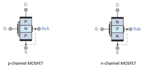
Where, D − Drain; G − Gate; S − Source; and Sub − Substrate
