- Analog Communication - Home
- Introduction
- Modulation
- Amplitude Modulation
- Numerical Problems 1
- AM Modulators
- AM Demodulators
- DSBSC Modulation
- DSBSC Modulators
- DSBSC Demodulators
- SSBSC Modulation
- SSBSC Modulators
- SSBSC Demodulator
- VSBSC Modulation
- Angle Modulation
- Numerical Problems 2
- FM Modulators
- FM Demodulators
- Multiplexing
- Noise
- SNR Calculations
- Transmitters
- Receivers
- Sampling
- Pulse Modulation
- Transducers
Analog Communication - Quick Guide
Analog Communication - Introduction
The word communication arises from the Latin word commnicre, which means to share. Communication is the basic step for exchange of information.
For example, a baby in a cradle, communicates with a cry when she needs her mother. A cow moos loudly when it is in danger. A person communicates with the help of a language. Communication is the bridge to share.
Communication can be defined as the process of exchange of information through means such as words, actions, signs, etc., between two or more individuals.
Parts of a Communication System
Any system, which provides communication consists of the three important and basic parts as shown in the following figure.
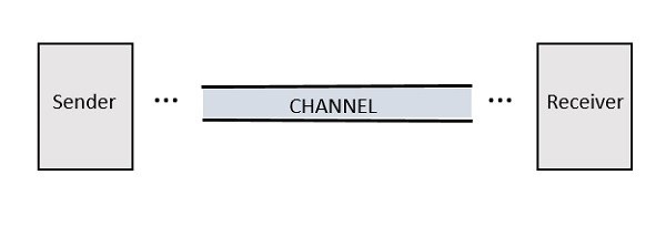
Sender is the person who sends a message. It could be a transmitting station from where the signal is transmitted.
Channel is the medium through which the message signals travel to reach the destination.
Receiver is the person who receives the message. It could be a receiving station where the transmitted signal is being received.
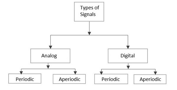
Types of Signals
Conveying an information by some means such as gestures, sounds, actions, etc., can be termed as signaling. Hence, a signal can be a source of energy which transmits some information. This signal helps to establish a communication between the sender and the receiver.
An electrical impulse or an electromagnetic wave which travels a distance to convey a message, can be termed as a signal in communication systems.
Depending on their characteristics, signals are mainly classified into two types: Analog and Digital. Analog and Digital signals are further classified, as shown in the following figure.
Analog Signal
A continuous time varying signal, which represents a time varying quantity can be termed as an Analog Signal. This signal keeps on varying with respect to time, according to the instantaneous values of the quantity, which represents it.
Example
Let us consider a tap that fills a tank of 100 liters capacity in an hour (6 AM to 7 AM). The portion of filling the tank is varied by the varying time. Which means, after 15 minutes (6:15 AM) the quarter portion of the tank gets filled, whereas at 6:45 AM, 3/4th of the tank is filled.
If we try to plot the varying portions of water in the tank according to the varying time, it would look like the following figure.
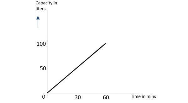
As the result shown in this image varies (increases) according to time, this time varying quantity can be understood as Analog quantity. The signal which represents this condition with an inclined line in the figure, is an Analog Signal. The communication based on analog signals and analog values is called as Analog Communication.
Digital Signal
A signal which is discrete in nature or which is non-continuous in form can be termed as a Digital signal. This signal has individual values, denoted separately, which are not based on the previous values, as if they are derived at that particular instant of time.
Example
Let us consider a classroom having 20 students. If their attendance in a week is plotted, it would look like the following figure.
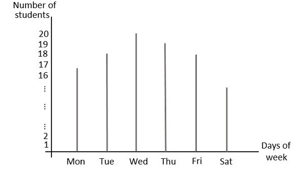
In this figure, the values are stated separately. For instance, the attendance of the class on Wednesday is 20 whereas on Saturday is 15. These values can be considered individually and separately or discretely, hence they are called as discrete values.
The binary digits which has only 1s and 0s are mostly termed as digital values. Hence, the signals which represent 1s and 0s are also called as digital signals. The communication based on digital signals and digital values is called as Digital Communication.
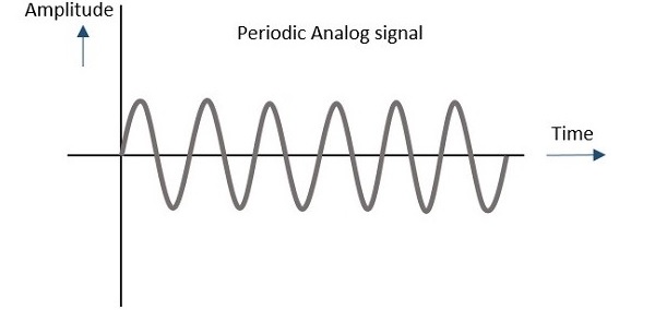
Periodic Signal
Any analog or digital signal, that repeats its pattern over a period of time, is called as a Periodic Signal. This signal has its pattern continued repeatedly and is easy to be assumed or to be calculated.
Example
If we consider a machinery in an industry, the process that takes place one after the other is a continuous procedure. For example, procuring and grading the raw material, processing the material in batches, packing a load of products one after the other, etc., follows a certain procedure repeatedly.
Such a process whether considered analog or digital, can be graphically represented as follows.
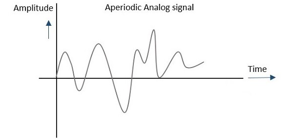
Aperiodic Signal
Any analog or digital signal, that doesnt repeat its pattern over a period of time is called as Aperiodic Signal. This signal has its pattern continued but the pattern is not repeated. It is also not so easy to be assumed or to be calculated.
Example
The daily routine of a person, if considered, consists of various types of work which take different time intervals for different tasks. The time interval or the work doesnt continuously repeat. For example, a person will not continuously brush his teeth from morning to night, that too with the same time period.
Such a process whether considered analog or digital, can be graphically represented as follows.
In general, the signals which are used in communication systems are analog in nature, which are transmitted in analog or converted to digital and then transmitted, depending upon the requirement.
Analog Communication - Modulation
For a signal to be transmitted to a distance, without the effect of any external interferences or noise addition and without getting faded away, it has to undergo a process called as Modulation. It improves the strength of the signal without disturbing the parameters of the original signal.
What is Modulation?
A message carrying a signal has to get transmitted over a distance and for it to establish a reliable communication, it needs to take the help of a high frequency signal which should not affect the original characteristics of the message signal.
The characteristics of the message signal, if changed, the message contained in it also alters. Hence, it is a must to take care of the message signal. A high frequency signal can travel up to a longer distance, without getting affected by external disturbances. We take the help of such high frequency signal which is called as a carrier signal to transmit our message signal. Such a process is simply called as Modulation.
Modulation is the process of changing the parameters of the carrier signal, in accordance with the instantaneous values of the modulating signal.
Need for Modulation
Baseband signals are incompatible for direct transmission. For such a signal, to travel longer distances, its strength has to be increased by modulating with a high frequency carrier wave, which doesnt affect the parameters of the modulating signal.
Advantages of Modulation
The antenna used for transmission, had to be very large, if modulation was not introduced. The range of communication gets limited as the wave cannot travel a distance without getting distorted.
Following are some of the advantages for implementing modulation in the communication systems.
- Reduction of antenna size
- No signal mixing
- Increased communication range
- Multiplexing of signals
- Possibility of bandwidth adjustments
- Improved reception quality
Signals in the Modulation Process
Following are the three types of signals in the modulation process.
Message or Modulating Signal
The signal which contains a message to be transmitted, is called as a message signal. It is a baseband signal, which has to undergo the process of modulation, to get transmitted. Hence, it is also called as the modulating signal.
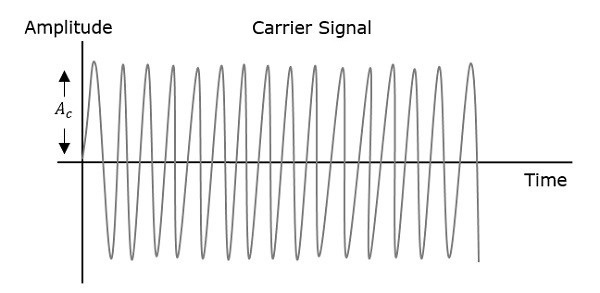
Carrier Signal
The high frequency signal, which has a certain amplitude, frequency and phase but contains no information is called as a carrier signal. It is an empty signal and is used to carry the signal to the receiver after modulation.
Modulated Signal
The resultant signal after the process of modulation is called as a modulated signal. This signal is a combination of modulating signal and carrier signal.
Types of Modulation
There are many types of modulations. Depending upon the modulation techniques used, they are classified as shown in the following figure.
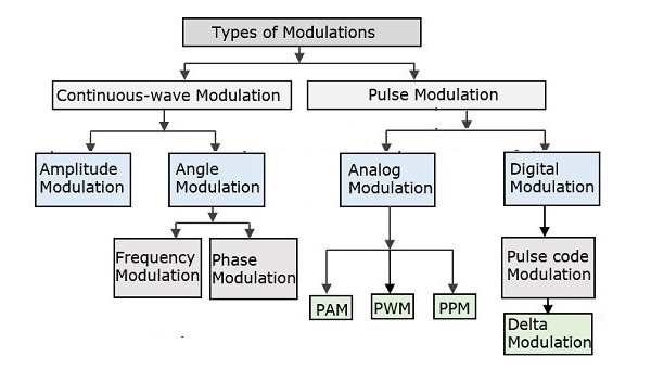
The types of modulations are broadly classified into continuous-wave modulation and pulse modulation.
Continuous-wave Modulation
In continuous-wave modulation, a high frequency sine wave is used as a carrier wave. This is further divided into amplitude and angle modulation.
If the amplitude of the high frequency carrier wave is varied in accordance with the instantaneous amplitude of the modulating signal, then such a technique is called as Amplitude Modulation.
If the angle of the carrier wave is varied, in accordance with the instantaneous value of the modulating signal, then such a technique is called as Angle Modulation. Angle modulation is further divided into frequency modulation and phase modulation.
If the frequency of the carrier wave is varied, in accordance with the instantaneous value of the modulating signal, then such a technique is called as Frequency Modulation.
If the phase of the high frequency carrier wave is varied in accordance with the instantaneous value of the modulating signal, then such a technique is called as Phase Modulation.
Pulse Modulation
In Pulse modulation, a periodic sequence of rectangular pulses, is used as a carrier wave. This is further divided into analog and digital modulation.
In analog modulation technique, if the amplitude or duration or position of a pulse is varied in accordance with the instantaneous values of the baseband modulating signal, then such a technique is called as Pulse Amplitude Modulation (PAM) or Pulse Duration/Width Modulation (PDM/PWM), or Pulse Position Modulation (PPM).
In digital modulation, the modulation technique used is Pulse Code Modulation (PCM) where the analog signal is converted into digital form of 1s and 0s. As the resultant is a coded pulse train, this is called as PCM. This is further developed as Delta Modulation (DM). These digital modulation techniques are discussed in our Digital Communications tutorial
Amplitude Modulation
A continuous-wave goes on continuously without any intervals and it is the baseband message signal, which contains the information. This wave has to be modulated.
According to the standard definition, The amplitude of the carrier signal varies in accordance with the instantaneous amplitude of the modulating signal. Which means, the amplitude of the carrier signal containing no information varies as per the amplitude of the signal containing information, at each instant. This can be well explained by the following figures.
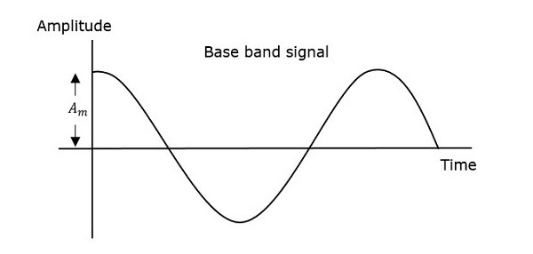
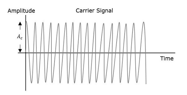

The first figure shows the modulating wave, which is the message signal. The next one is the carrier wave, which is a high frequency signal and contains no information. While, the last one is the resultant modulated wave.
It can be observed that the positive and negative peaks of the carrier wave, are interconnected with an imaginary line. This line helps recreating the exact shape of the modulating signal. This imaginary line on the carrier wave is called as Envelope. It is the same as that of the message signal.
Mathematical Expressions
Following are the mathematical expressions for these waves.
Time-domain Representation of the Waves
Let the modulating signal be,
$$m\left ( t \right )=A_m\cos\left ( 2\pi f_mt \right )$$
and the carrier signal be,
$$c\left ( t \right )=A_c\cos\left ( 2\pi f_ct \right )$$
Where,
$A_m$ and $A_c$ are the amplitude of the modulating signal and the carrier signal respectively.
$f_m$ and $f_c$ are the frequency of the modulating signal and the carrier signal respectively.
Then, the equation of Amplitude Modulated wave will be
$s(t)= \left [ A_c+A_m\cos\left ( 2\pi f_mt \right ) \right ]\cos \left ( 2\pi f_ct \right )$ (Equation 1)
Modulation Index
A carrier wave, after being modulated, if the modulated level is calculated, then such an attempt is called as Modulation Index or Modulation Depth. It states the level of modulation that a carrier wave undergoes.
Rearrange the Equation 1 as below.
$s(t)=A_c\left [ 1+\left ( \frac{A_m}{A_c} \right )\cos \left ( 2\pi f_mt \right ) \right ]\cos \left ( 2\pi f_ct \right )$
$\Rightarrow s\left ( t \right ) = A_c\left [ 1 + \mu \cos \left ( 2 \pi f_m t \right ) \right ] \cos\left ( 2 \pi f_ct \right )$ (Equation 2)
Where, $\mu$ is Modulation index and it is equal to the ratio of $A_m$ and $A_c$. Mathematically, we can write it as
$\mu = \frac{A_m}{A_c}$ (Equation 3)
Hence, we can calculate the value of modulation index by using the above formula, when the amplitudes of the message and carrier signals are known.
Now, let us derive one more formula for Modulation index by considering Equation 1. We can use this formula for calculating modulation index value, when the maximum and minimum amplitudes of the modulated wave are known.
Let $A_\max$ and $A_\min$ be the maximum and minimum amplitudes of the modulated wave.
We will get the maximum amplitude of the modulated wave, when $\cos \left ( 2\pi f_mt \right )$ is 1.
$\Rightarrow A_\max = A_c + A_m$ (Equation 4)
We will get the minimum amplitude of the modulated wave, when $\cos \left ( 2\pi f_mt \right )$ is -1.
$\Rightarrow A_\min = A_c - A_m$ (Equation 5)
Add Equation 4 and Equation 5.
$$A_\max + A_\min = A_c+A_m+A_c-A_m = 2A_c$$
$\Rightarrow A_c = \frac{A_\max + A_\min}{2}$ (Equation 6)
Subtract Equation 5 from Equation 4.
$$A_\max - A_\min = A_c + A_m - \left (A_c -A_m \right )=2A_m$$
$\Rightarrow A_m = \frac{A_\max - A_\min}{2}$ (Equation 7)
The ratio of Equation 7 and Equation 6 will be as follows.
$$\frac{A_m}{A_c} = \frac{\left ( A_{max} - A_{min}\right )/2}{\left ( A_{max} + A_{min}\right )/2}$$
$\Rightarrow \mu = \frac{A_\max - A_\min}{A_\max + A_\min}$ (Equation 8)
Therefore, Equation 3 and Equation 8 are the two formulas for Modulation index. The modulation index or modulation depth is often denoted in percentage called as Percentage of Modulation. We will get the percentage of modulation, just by multiplying the modulation index value with 100.
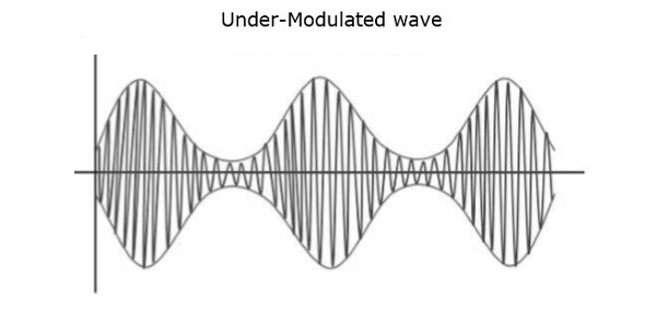
For a perfect modulation, the value of modulation index should be 1, which implies the percentage of modulation should be 100%.
For instance, if this value is less than 1, i.e., the modulation index is 0.5, then the modulated output would look like the following figure. It is called as Under-modulation. Such a wave is called as an under-modulated wave.
If the value of the modulation index is greater than 1, i.e., 1.5 or so, then the wave will be an over-modulated wave. It would look like the following figure.
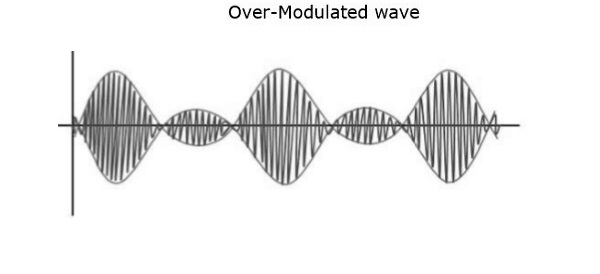
As the value of the modulation index increases, the carrier experiences a 180o phase reversal, which causes additional sidebands and hence, the wave gets distorted. Such an over-modulated wave causes interference, which cannot be eliminated.
Bandwidth of AM Wave
Bandwidth (BW) is the difference between the highest and lowest frequencies of the signal. Mathematically, we can write it as
$$BW = f_{max} - f_{min}$$
Consider the following equation of amplitude modulated wave.
$$s\left ( t \right ) = A_c\left [ 1 + \mu \cos \left ( 2 \pi f_m t \right ) \right ] \cos\left ( 2 \pi f_ct \right )$$
$$\Rightarrow s\left ( t \right ) = A_c\cos \left ( 2\pi f_ct \right )+ A_c\mu \cos(2\pi f_ct)\cos \left ( 2\pi f_mt \right )$$
$\Rightarrow s\left ( t \right )= A_c\cos \left ( 2\pi f_ct \right )+\frac{A_c\mu }{2}\cos \left [ 2\pi \left ( f_c+f_m \right ) t\right ]+\frac{A_c\mu }{2}\cos \left [ 2\pi \left ( f_c-f_m \right ) t\right ]$
Hence, the amplitude modulated wave has three frequencies. Those are carrier frequency $f_c$, upper sideband frequency $f_c + f_m$ and lower sideband frequency $f_c-f_m$
Here,
$f_{max}=f_c+f_m$ and $f_{min}=f_c-f_m$
Substitute, $f_{max}$ and $f_{min}$ values in bandwidth formula.
$$BW=f_c+f_m-\left ( f_c-f_m \right )$$
$$\Rightarrow BW=2f_m$$
Thus, it can be said that the bandwidth required for amplitude modulated wave is twice the frequency of the modulating signal.
Power Calculations of AM Wave
Consider the following equation of amplitude modulated wave.
$\ s\left ( t \right )= A_c\cos \left ( 2\pi f_ct \right )+\frac{A_c\mu }{2}\cos \left [ 2\pi \left ( f_c+f_m \right ) t\right ]+\frac{A_c\mu }{2}\cos \left [ 2\pi \left ( f_c-f_m \right ) t\right ]$
Power of AM wave is equal to the sum of powers of carrier, upper sideband, and lower sideband frequency components.
$$P_t=P_c+P_{USB}+P_{LSB}$$
We know that the standard formula for power of cos signal is
$$P=\frac{{v_{rms}}^{2}}{R}=\frac{\left ( v_m/ \sqrt{2}\right )^2}{2}$$
Where,
$v_{rms}$ is the rms value of cos signal.
$v_m$ is the peak value of cos signal.
First, let us find the powers of the carrier, the upper and lower sideband one by one.
Carrier power
$$P_c=\frac{\left ( A_c/\sqrt{2} \right )^2}{R}=\frac{{A_{c}}^{2}}{2R}$$
Upper sideband power
$$P_{USB}=\frac{\left ( A_c\mu /2\sqrt{2} \right )^2}{R}=\frac{{A_{c}}^{2}{_{\mu }}^{2}}{8R}$$
Similarly, we will get the lower sideband power same as that of the upper side band power.
$$P_{LSB}=\frac{{A_{c}}^{2}{_{\mu }}^{2}}{8R}$$
Now, let us add these three powers in order to get the power of AM wave.
$$P_t=\frac{{A_{c}}^{2}}{2R}+\frac{{A_{c}}^{2}{_{\mu }}^{2}}{8R}+\frac{{A_{c}}^{2}{_{\mu }}^{2}}{8R}$$
$$\Rightarrow P_t=\left ( \frac{{A_{c}}^{2}}{2R} \right )\left ( 1+\frac{\mu ^2}{4}+\frac{\mu ^2}{4} \right )$$
$$\Rightarrow P_t=P_c\left ( 1+\frac{\mu ^2}{2} \right )$$
We can use the above formula to calculate the power of AM wave, when the carrier power and the modulation index are known.
If the modulation index $\mu=1$ then the power of AM wave is equal to 1.5 times the carrier power. So, the power required for transmitting an AM wave is 1.5 times the carrier power for a perfect modulation.
Numerical Problems 1
In the previous chapter, we have discussed the parameters used in Amplitude Modulation. Each parameter has its own formula. By using those formulas, we can find the respective parameter values. In this chapter, let us solve a few problems based on the concept of amplitude modulation.
Problem 1
A modulating signal $m\left ( t \right )=10 \cos \left ( 2\pi \times 10^3 t\right )$ is amplitude modulated with a carrier signal $c\left ( t \right )=50 \cos \left ( 2\pi \times 10^5 t\right )$. Find the modulation index, the carrier power, and the power required for transmitting AM wave.
Solution
Given, the equation of modulating signal as
$$m\left ( t \right )=10\cos \left ( 2\pi \times 10^3 t\right )$$
We know the standard equation of modulating signal as
$$m\left ( t \right )=A_m\cos\left ( 2\pi f_mt \right )$$
By comparing the above two equations, we will get
Amplitude of modulating signal as $A_m=10 volts$
and Frequency of modulating signal as $$f_m=10^3 Hz=1 KHz$$
Given, the equation of carrier signal is
$$c\left ( t \right )=50\cos \left ( 2\pi \times 10^5t \right )$$
The standard equation of carrier signal is
$$c\left ( t \right )=A_c\cos\left ( 2\pi f_ct \right )$$
By comparing these two equations, we will get
Amplitude of carrier signal as $A_c=50volts$
and Frequency of carrier signal as $f_c=10^5 Hz=100 KHz$
We know the formula for modulation index as
$$\mu =\frac{A_m}{A_c}$$
Substitute, $A_m$ and $A_c$ values in the above formula.
$$\mu=\frac{10}{50}=0.2$$
Therefore, the value of modulation index is 0.2 and percentage of modulation is 20%.
The formula for Carrier power, $P_c=$ is
$$P_c=\frac{{A_{c}}^{2}}{2R}$$
Assume $R=1\Omega$ and substitute $A_c$ value in the above formula.
$$P_c=\frac{\left ( 50 \right )^2}{2\left ( 1 \right )}=1250W$$
Therefore, the Carrier power, $P_c$ is 1250 watts.
We know the formula for power required for transmitting AM wave is
$$\Rightarrow P_t=P_c\left ( 1+\frac{\mu ^2}{2} \right )$$
Substitute $P_c$ and $\mu$ values in the above formula.
$$P_t=1250\left ( 1+\frac{\left ( 0.2 \right )^2}{2} \right )=1275W$$
Therefore, the power required for transmitting AM wave is 1275 watts.
Problem 2
The equation of amplitude wave is given by $s\left ( t \right ) = 20\left [ 1 + 0.8 \cos \left ( 2\pi \times 10^3t \right ) \right ]\cos \left ( 4\pi \times 10^5t \right )$. Find the carrier power, the total sideband power, and the band width of AM wave.
Solution
Given, the equation of Amplitude modulated wave is
$$s\left ( t \right )=20\left [ 1+0.8 \cos\left ( 2\pi \times 10^3t \right ) \right ]\cos \left ( 4\pi \times 10^5t \right )$$
Re-write the above equation as
$$s\left ( t \right )=20\left [ 1+0.8 \cos\left ( 2\pi \times 10^3t \right ) \right ]\cos \left ( 2\pi \times 2 \times 10^5t \right )$$
We know the equation of Amplitude modulated wave is
$$s\left ( t \right )=A_c\left [ 1+\mu \cos\left ( 2\pi f_mt \right ) \right ]\cos\left ( 2 \pi f_ct \right )$$
By comparing the above two equations, we will get
Amplitude of carrier signal as $A_c=20 volts$
Modulation index as $\mu=0.8$
Frequency of modulating signal as $f_m=10^3Hz=1 KHz$
Frequency of carrier signal as $f_c=2\times 10^5Hz=200KHz$
The formula for Carrier power, $P_c$is
$$P_c=\frac{{A_{e}}^{2}}{2R}$$
Assume $R=1\Omega$ and substitute $A_c$ value in the above formula.
$$P_c=\frac{\left ( 20 \right )^2}{2\left ( 1 \right )}=200W$$
Therefore, the Carrier power, $P_c$ is 200watts.
We know the formula for total side band power is
$$P_{SB}=\frac{P_c\mu^2}{2}$$
Substitute $P_c$ and $\mu$ values in the above formula.
$$P_{SB}=\frac{200\times \left ( 0.8 \right )^2}{2}=64W$$
Therefore, the total side band power is 64 watts.
We know the formula for bandwidth of AM wave is
$$BW=2f_m$$
Substitute $f_m$ value in the above formula.
$$BW=2\left ( 1K \right )=2 KHz$$
Therefore, the bandwidth of AM wave is 2 KHz.
Analog Communication - AM Modulators
In this chapter, let us discuss about the modulators, which generate amplitude modulated wave. The following two modulators generate AM wave.
- Square law modulator
- Switching modulator
Square Law Modulator
Following is the block diagram of the square law modulator
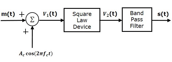
Let the modulating and carrier signals be denoted as $m\left ( t \right )$ and $A\cos\left ( 2\pi f_ct\right )$ respectively. These two signals are applied as inputs to the summer (adder) block. This summer block produces an output, which is the addition of the modulating and the carrier signal. Mathematically, we can write it as
$$V_1t=m\left ( t \right )+A_c\cos\left ( 2 \pi f_ct \right )$$
This signal $V_1t$ is applied as an input to a nonlinear device like diode. The characteristics of the diode are closely related to square law.
$V_2t=k_1V_1\left ( t \right )+k_2V_1^2\left ( t \right )$(Equation 1)
Where, $k_1$ and $k_2$ are constants.
Substitute $V_1\left (t \right )$ in Equation 1
$$V_2\left (t\right ) = k_1\left [ m\left ( t \right ) + A_c \cos \left ( 2 \pi f_ct \right ) \right ] + k_2\left [ m\left ( t \right ) + A_c \cos\left ( 2 \pi f_ct \right ) \right ]^2$$
$\Rightarrow V_2\left (t\right ) = k_1 m\left ( t \right ) +k_1 A_c \cos \left ( 2 \pi f_ct \right ) +k_2 m^2\left ( t \right ) +$
$ k_2A_c^2 \cos^2\left ( 2 \pi f_ct \right )+2k_2m\left ( t \right )A_c \cos\left ( 2 \pi f_ct \right )$
$\Rightarrow V_2\left (t\right ) = k_1 m\left ( t \right ) +k_2 m^2\left ( t \right ) +k_2 A^2_c \cos^2 \left ( 2 \pi f_ct \right ) +$
$k_1A_c\left [ 1+\left ( \frac{2k_2}{k_1} \right )m\left ( t \right ) \right ] \cos\left ( 2 \pi f_ct \right )$
The last term of the above equation represents the desired AM wave and the first three terms of the above equation are unwanted. So, with the help of band pass filter, we can pass only AM wave and eliminate the first three terms.
Therefore, the output of square law modulator is
$$s\left ( t \right )=k_1A_c\left [1+\left ( \frac{2k_2}{k_1} \right ) m\left ( t \right ) \right ] \cos\left ( 2 \pi f_ct \right )$$
The standard equation of AM wave is
$$s\left ( t \right )=A_c\left [ 1+k_am\left ( t \right ) \right ] \cos \left (2 \pi f_ct \right )$$
Where, $K_a$ is the amplitude sensitivity
By comparing the output of the square law modulator with the standard equation of AM wave, we will get the scaling factor as $k_1$ and the amplitude sensitivity $k_a$ as $\frac{2k_2}{k1}$.
Switching Modulator
Following is the block diagram of switching modulator.
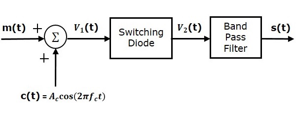
Switching modulator is similar to the square law modulator. The only difference is that in the square law modulator, the diode is operated in a non-linear mode, whereas, in the switching modulator, the diode has to operate as an ideal switch.
Let the modulating and carrier signals be denoted as $m\left ( t \right )$ and $c\left ( t \right )= A_c \cos\left ( 2\pi f_ct \right )$ respectively. These two signals are applied as inputs to the summer (adder) block. Summer block produces an output, which is the addition of modulating and carrier signals. Mathematically, we can write it as
$$V_1\left ( t \right )=m\left ( t \right )+c\left ( t \right )= m\left ( t \right )+A_c \cos\left ( 2 \pi f_ct \right )$$
This signal $V_1\left ( t \right )$ is applied as an input of diode. Assume, the magnitude of the modulating signal is very small when compared to the amplitude of carrier signal $A_c$. So, the diodes ON and OFF action is controlled by carrier signal $c\left ( t \right )$. This means, the diode will be forward biased when $c\left ( t \right )> 0$ and it will be reverse biased when $c\left ( t \right )
Therefore, the output of the diode is
$$V_2 \left ( t \right )=\left\{\begin{matrix} V_1\left ( t \right )& if &c\left ( t \right )>0 \\ 0& if & c\left ( t \right )
We can approximate this as
$V_2\left ( t \right ) = V_1\left ( t \right )x\left ( t \right )$(Equation 2)
Where, $x\left ( t \right )$ is a periodic pulse train with time period $T=\frac{1}{f_c}$
The Fourier series representation of this periodic pulse train is
$$x\left ( t \right )=\frac{1}{2}+\frac{2}{\pi }\sum_{n=1}^{\infty}\frac{\left ( -1 \right )^n-1}{2n-1} \cos\left (2 \pi \left ( 2n-1 \right ) f_ct \right )$$
$$\Rightarrow x\left ( t \right )=\frac{1}{2}+\frac{2}{\pi} \cos\left ( 2 \pi f_ct \right )-\frac{2}{3\pi } \cos\left ( 6 \pi f_ct \right ) +....$$
Substitute, $V_1\left ( t \right )$ and $x\left ( t \right )$ values in Equation 2.
$V_2\left ( t \right )=\left [ m\left ( t \right )+A_c \cos\left ( 2 \pi f_ct \right ) \right ] \left [ \frac{1}{2} + \frac{2}{\pi} \cos \left ( 2 \pi f_ct \right )-\frac{2}{3\pi} \cos\left ( 6 \pi f_ct \right )+.....\right ]$
$V_2\left ( t \right )=\frac{m\left ( t \right )}{2}+\frac{A_c}{2} \cos\left ( 2 \pi f_ct \right )+\frac{2m\left ( t \right )}{\pi} \cos\left ( 2 \pi f_ct \right ) +\frac{2A_c}{\pi} \cos^2\left ( 2 \pi f_ct \right )-$
$\frac{2m\left ( t \right )}{3\pi} \cos\left ( 6 \pi f_ct \right )-\frac{2A_c}{3\pi}\cos \left ( 2 \pi f_ct \right ) \cos\left ( 6 \pi f_ct \right )+..... $
$V_2\left ( t \right )=\frac{A_c}{2}\left ( 1+\left ( \frac{4}{\pi A_c} \right )m\left ( t \right ) \right ) \cos\left ( 2 \pi f_ct \right ) + \frac{m\left ( t \right )}{2}+\frac{2A_c}{\pi} \cos^2\left ( 2 \pi f_ct \right )-$
$\frac{2m\left ( t \right )}{3 \pi} \cos\left ( 6 \pi f_ct \right )-\frac{2A_c}{3\pi} \cos\left ( 2 \pi f_ct \right ) \cos\left ( 6 \pi f_ct \right )+.....$
The 1st term of the above equation represents the desired AM wave and the remaining terms are unwanted terms. Thus, with the help of band pass filter, we can pass only AM wave and eliminate the remaining terms.
Therefore, the output of switching modulator is
$$s\left ( t \right )=\frac{A_c}{2}\left ( 1+\left ( \frac{4}{\pi A_c} \right ) m\left ( t \right )\right ) \cos\left ( 2 \pi f_ct \right )$$
We know the standard equation of AM wave is
$$s\left ( t \right )=A_c\left [ 1+k_am\left ( t \right ) \right ] \cos\left ( 2 \pi f_ct \right )$$
Where, $k_a$ is the amplitude sensitivity.
By comparing the output of the switching modulator with the standard equation of AM wave, we will get the scaling factor as 0.5 and amplitude sensitivity $k_a$ as $\frac{4}{\pi A_c}$ .
Analog Communication - AM Demodulators
The process of extracting an original message signal from the modulated wave is known as detection or demodulation. The circuit, which demodulates the modulated wave is known as the demodulator. The following demodulators (detectors) are used for demodulating AM wave.
- Square Law Demodulator
- Envelope Detector
Square Law Demodulator
Square law demodulator is used to demodulate low level AM wave. Following is the block diagram of thesquare law demodulator.
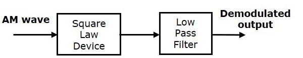
This demodulator contains a square law device and low pass filter. The AM wave $V_1\left ( t \right )$ is applied as an input to this demodulator.
The standard form of AM wave is
$$V_1\left ( t \right )=A_c\left [ 1+k_am\left ( t \right ) \right ] \cos\left ( 2 \pi f_ct \right )$$
We know that the mathematical relationship between the input and the output of square law device is
$V_2\left ( t \right )=k_1V_1\left ( t \right )+k_2V_1^2\left ( t \right )$(Equation 1)
Where,
$V_1\left ( t \right )$ is the input of the square law device, which is nothing but the AM wave
$V_2\left ( t \right )$ is the output of the square law device
$k_1$ and $k_2$ are constants
Substitute $V_1\left ( t \right )$ in Equation 1
$$V_2\left ( t \right )=k_1\left ( A_c\left [ 1+k_am\left ( t \right ) \right ] \cos\left ( 2 \pi f_ct \right )\right )+k_2\left ( A_c\left [ 1+k_am\left ( t \right ) \right ] \cos\left ( 2 \pi f_ct \right )\right )^2$$
$\Rightarrow V_2\left ( t \right )=k_1A_c \cos \left ( 2 \pi f_ct \right )+k_1A_ck_am\left ( t \right ) \cos \left ( 2 \pi f_ct \right )+$
$k_2{A_{c}}^{2}\left [ 1+{K_{a}}^{2}m^2\left ( t \right )+2k_am\left ( t \right ) \right ]\left ( \frac{1+ \cos\left ( 4 \pi f_ct \right )}{2} \right )$
$\Rightarrow V_2\left ( t \right )=k_1A_c \cos \left ( 2 \pi f_ct \right )+k_1A_ck_am\left ( t \right ) \cos \left ( 2 \pi f_ct \right)+\frac{K_2{A_{c}}^{2}}{2}+$
$\frac{K_2{A_{c}}^{2}}{2} \cos \left ( 4 \pi f_ct \right )+\frac{k_2 {A_{c}}^{2}{k_{a}}^{2}m^2\left ( t \right )}{2}+\frac{k_2 {A_{c}}^{2}{k_{a}}^{2}m^2\left ( t \right )}{2} \cos\left ( 4 \pi f_ct \right )+$
$k_2{A_{c}}^{2}k_am\left ( t \right )+k_2{A_{c}}^{2}k_am\left ( t \right )\cos \left ( 4 \pi f_ct \right )$
In the above equation, the term $k_2{A_{c}}^{2}k_am\left ( t \right )$ is the scaled version of the message signal. It can be extracted by passing the above signal through a low pass filter and the DC component $\frac{k_2{A_{c}}^{2}}{2}$ can be eliminated with the help of a coupling capacitor.
Envelope Detector
Envelope detector is used to detect (demodulate) high level AM wave. Following is the block diagram of the envelope detector.
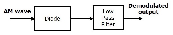
This envelope detector consists of a diode and low pass filter. Here, the diode is the main detecting element. Hence, the envelope detector is also called as the diode detector. The low pass filter contains a parallel combination of the resistor and the capacitor.
The AM wave $s\left ( t \right )$ is applied as an input to this detector.
We know the standard form of AM wave is
$$s\left ( t \right )=A_c\left [ 1+k_am\left ( t \right ) \right ] \cos\left ( 2 \pi f_ct \right )$$
In the positive half cycle of AM wave, the diode conducts and the capacitor charges to the peak value of AM wave. When the value of AM wave is less than this value, the diode will be reverse biased. Thus, the capacitor will discharge through resistor R till the next positive half cycle of AM wave. When the value of AM wave is greater than the capacitor voltage, the diode conducts and the process will be repeated.
We should select the component values in such a way that the capacitor charges very quickly and discharges very slowly. As a result, we will get the capacitor voltage waveform same as that of the envelope of AM wave, which is almost similar to the modulating signal.
Analog Communication - DSBSC Modulation
In the process of Amplitude Modulation, the modulated wave consists of the carrier wave and two sidebands. The modulated wave has the information only in the sidebands. Sideband is nothing but a band of frequencies, containing power, which are the lower and higher frequencies of the carrier frequency.
The transmission of a signal, which contains a carrier along with two sidebands can be termed as Double Sideband Full Carrier system or simply DSBFC. It is plotted as shown in the following figure.
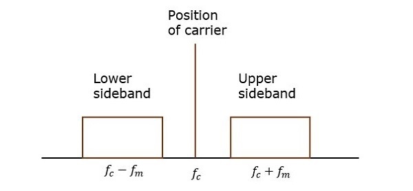
However, such a transmission is inefficient. Because, two-thirds of the power is being wasted in the carrier, which carries no information.
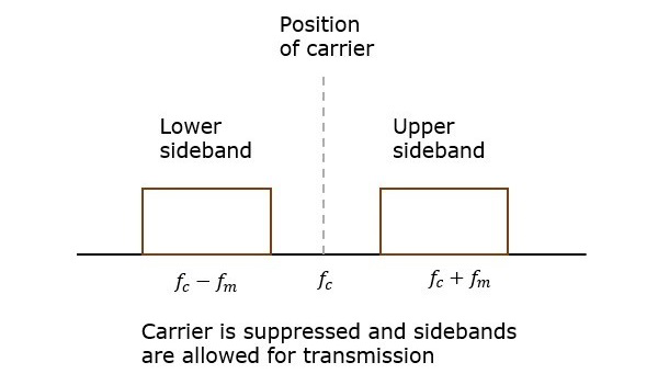
If this carrier is suppressed and the saved power is distributed to the two sidebands, then such a process is called as Double Sideband Suppressed Carrier system or simply DSBSC. It is plotted as shown in the following figure.
Mathematical Expressions
Let us consider the same mathematical expressions for modulating and carrier signals as we have considered in the earlier chapters.
i.e., Modulating signal
$$m\left ( t \right )=A_m \cos \left ( 2 \pi f_mt\right )$$
Carrier signal
$$c\left ( t \right )=A_c \cos \left ( 2 \pi f_ct\right )$$
Mathematically, we can represent the equation of DSBSC wave as the product of modulating and carrier signals.
$$s\left ( t \right )=m\left ( t \right )c\left ( t \right )$$
$$\Rightarrow s\left ( t \right )=A_mA_c \cos \left ( 2 \pi f_mt \right )\cos \left ( 2 \pi f_ct \right )$$
Bandwidth of DSBSC Wave
We know the formula for bandwidth (BW) is
$$BW=f_{max}-f_{min}$$
Consider the equation of DSBSC modulated wave.
$$s\left ( t \right )=A_mA_c \cos\left ( 2 \pi f_mt \right ) \cos(2 \pi f_ct)$$
$$\Rightarrow s\left ( t \right )=\frac{A_mA_c}{2} \cos\left [ 2 \pi\left ( f_c+f_m \right ) t\right ]+\frac{A_mA_c}{2} \cos\left [ 2 \pi\left ( f_c-f_m \right ) t\right ]$$
The DSBSC modulated wave has only two frequencies. So, the maximum and minimum frequencies are $f_c+f_m$ and $f_c-f_m$ respectively.
i.e.,
$f_{max}=f_c+f_m$ and $f_{min}=f_c-f_m$
Substitute, $f_{max}$ and $f_{min}$ values in the bandwidth formula.
$$BW=f_c+f_m-\left ( f_c-f_m \right )$$
$$\Rightarrow BW=2f_m$$
Thus, the bandwidth of DSBSC wave is same as that of AM wave and it is equal to twice the frequency of the modulating signal.
Power Calculations of DSBSC Wave
Consider the following equation of DSBSC modulated wave.
$$s\left ( t \right )=\frac{A_mA_c}{2} \cos\left [ 2 \pi \left ( f_c+f_m \right ) t\right ]+\frac{A_mA_c}{2} \cos\left [ 2 \pi \left ( f_c-f_m \right ) t\right ]$$
Power of DSBSC wave is equal to the sum of powers of upper sideband and lower sideband frequency components.
$$P_t=P_{USB}+P_{LSB}$$
We know the standard formula for power of cos signal is
$$P=\frac{{v_{rms}}^{2}}{R}=\frac{\left ( v_m\sqrt{2}\right )^2}{R}$$
First, let us find the powers of upper sideband and lower sideband one by one.
Upper sideband power
$$P_{USB}=\frac{\left ( A_mA_c / 2\sqrt{2}\right )^2}{R}=\frac{{A_{m}}^{2}{A_{c}}^{2}}{8R}$$
Similarly, we will get the lower sideband power same as that of upper sideband power.
$$P_{USB}=\frac{{A_{m}}^{2}{A_{c}}^{2}}{8R}$$
Now, let us add these two sideband powers in order to get the power of DSBSC wave.
$$P_t=\frac{{A_{m}}^{2}{A_{c}}^{2}}{8R}+\frac{{A_{m}}^{2}{A_{c}}^{2}}{8R}$$
$$\Rightarrow P_t=\frac{{A_{m}}^{2}{A_{c}}^{2}}{4R}$$
Therefore, the power required for transmitting DSBSC wave is equal to the power of both the sidebands.
Analog Communication - DSBSC Modulators
In this chapter, let us discuss about the modulators, which generate DSBSC wave. The following two modulators generate DSBSC wave.
- Balanced modulator
- Ring modulator
Balanced Modulator
Following is the block diagram of the Balanced modulator.
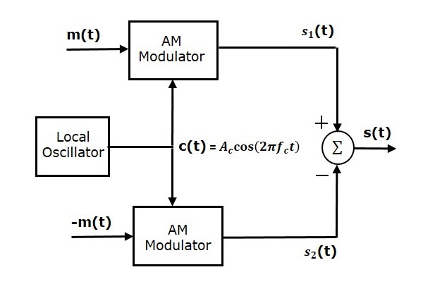
Balanced modulator consists of two identical AM modulators. These two modulators are arranged in a balanced configuration in order to suppress the carrier signal. Hence, it is called as Balanced modulator.
The same carrier signal $c\left ( t \right )= A_c \cos \left ( 2 \pi f_ct \right )$ is applied as one of the inputs to these two AM modulators. The modulating signal $m\left ( t \right )$ is applied as another input to the upper AM modulator. Whereas, the modulating signal $m\left ( t \right )$ with opposite polarity, i.e., $-m\left ( t \right )$ is applied as another input to the lower AM modulator.
Output of the upper AM modulator is
$$s_1\left ( t \right )=A_c\left [1+k_am\left ( t \right ) \right ] \cos\left ( 2 \pi f_ct \right )$$
Output of the lower AM modulator is
$$s_2\left ( t \right )=A_c\left [1-k_am\left ( t \right ) \right ] \cos\left ( 2 \pi f_ct \right )$$
We get the DSBSC wave $s\left ( t \right )$ by subtracting $s_2\left ( t \right )$ from $s_1\left ( t \right )$. The summer block is used to perform this operation. $s_1\left ( t \right )$ with positive sign and $s_2\left ( t \right )$ with negative sign are applied as inputs to summer block. Thus, the summer block produces an output $s\left ( t \right )$ which is the difference of $s_1\left ( t \right )$ and $s_2\left ( t \right )$.
$$\Rightarrow s\left ( t \right )=A_c\left [ 1+k_am\left ( t \right ) \right ] \cos\left ( 2 \pi f_ct \right )-A_c\left [ 1-k_am\left ( t \right ) \right ] \cos\left ( 2 \pi f_ct \right )$$
$$\Rightarrow s\left ( t \right )=A_c \cos\left ( 2 \pi f_ct \right )+A_ck_am\left ( t \right ) \cos\left ( 2 \pi f_ct \right )- A_c \cos\left ( 2 \pi f_ct \right )+$$
$A_ck_am\left ( t \right ) \cos\left ( 2 \pi f_ct \right )$
$\Rightarrow s\left ( t \right )=2A_ck_am\left ( t \right ) \cos\left ( 2 \pi f_ct \right )$
We know the standard equation of DSBSC wave is
$$s\left ( t \right )=A_cm \left ( t \right ) \cos\left ( 2 \pi f_ct \right )$$
By comparing the output of summer block with the standard equation of DSBSC wave, we will get the scaling factor as $2k_a$
Ring Modulator
Following is the block diagram of the Ring modulator.
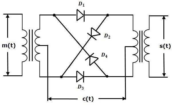
In this diagram, the four diodes $D_1$,$D_2$,$D_3$ and $D_4$ are connected in the ring structure. Hence, this modulator is called as the ring modulator. Two center tapped transformers are used in this diagram. The message signal $m\left ( t \right )$ is applied to the input transformer. Whereas, the carrier signals $c\left ( t \right )$ is applied between the two center tapped transformers.
For positive half cycle of the carrier signal, the diodes $D_1$ and $D_3$ are switched ON and the other two diodes $D_2$ and $D_4$ are switched OFF. In this case, the message signal is multiplied by +1.
For negative half cycle of the carrier signal, the diodes $D_2$ and $D_4$ are switched ON and the other two diodes $D_1$ and $D_3$ are switched OFF. In this case, the message signal is multiplied by -1. This results in $180^0$ phase shift in the resulting DSBSC wave.
From the above analysis, we can say that the four diodes $D_1$, $D_2$, $D_3$ and $D_4$ are controlled by the carrier signal. If the carrier is a square wave, then the Fourier series representation of $c\left ( t \right )$ is represented as
$$c\left ( t \right )=\frac{4}{\pi}\sum_{n=1}^{\infty }\frac{\left ( -1 \right )^{n-1}}{2n-1} \cos\left [2 \pi f_ct\left ( 2n-1 \right ) \right ]$$
We will get DSBSC wave $s\left ( t \right )$, which is just the product of the carrier signal $c\left ( t \right )$ and the message signal $m\left ( t \right )$ i.e.,
$$s\left ( t \right )=\frac{4}{\pi}\sum_{n=1}^{\infty }\frac{\left ( -1 \right )^{n-1}}{2n-1} \cos\left [2 \pi f_ct\left ( 2n-1 \right ) \right ]m\left ( t \right )$$
The above equation represents DSBSC wave, which is obtained at the output transformer of the ring modulator.
DSBSC modulators are also called as product modulators as they produce the output, which is the product of two input signals.
DSBSC Demodulators
The process of extracting an original message signal from DSBSC wave is known as detection or demodulation of DSBSC. The following demodulators (detectors) are used for demodulating DSBSC wave.
- Coherent Detector
- Costas Loop
Coherent Detector
Here, the same carrier signal (which is used for generating DSBSC signal) is used to detect the message signal. Hence, this process of detection is called as coherent or synchronous detection. Following is the block diagram of the coherent detector.
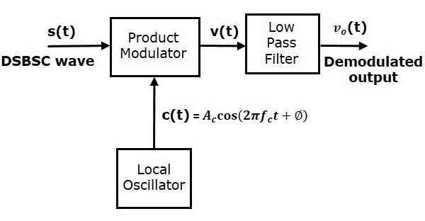
In this process, the message signal can be extracted from DSBSC wave by multiplying it with a carrier, having the same frequency and the phase of the carrier used in DSBSC modulation. The resulting signal is then passed through a Low Pass Filter. Output of this filter is the desired message signal.
Let the DSBSC wave be
$$s\left ( t \right )= A_c \cos\left ( 2 \pi f_ct \right )m \left ( t \right )$$
The output of the local oscillator is
$$c\left ( t \right )= A_c \cos\left ( 2 \pi f_ct+ \phi \right )$$
Where, $\phi$ is the phase difference between the local oscillator signal and the carrier signal, which is used for DSBSC modulation.
From the figure, we can write the output of product modulator as
$$v\left ( t \right )=s\left ( t \right )c\left ( t \right )$$
Substitute, $s\left ( t \right )$ and $c\left ( t \right )$ values in the above equation.
$$\Rightarrow v\left ( t \right )=A_c \cos \left ( 2 \pi f_ct \right )m\left ( t \right )A_c \cos \left ( 2 \pi f_ct + \phi \right )$$
$={A_{c}}^{2} \cos \left ( 2 \pi f_ct \right ) \cos \left ( 2 \pi f_ct + \phi \right )m\left ( t \right )$
$=\frac{{A_{c}}^{2}}{2}\left [ \cos\left ( 4 \pi f_ct+ \phi \right )+ \cos \phi \right ]m\left ( t \right )$
$$v\left ( t \right )=\frac{{A_{c}}^{2}}{2} \cos\phi m\left ( t \right )+\frac{{A_{c}}^{2}}{2} \cos \left ( 4 \pi f_ct+ \phi \right )m\left ( t \right )$$
In the above equation, the first term is the scaled version of the message signal. It can be extracted by passing the above signal through a low pass filter.
Therefore, the output of low pass filter is
$$v_0t=\frac{{A_{c}}^{2}}{2} \cos \phi m \left ( t \right )$$
The demodulated signal amplitude will be maximum, when $\phi=0^0$. Thats why the local oscillator signal and the carrier signal should be in phase, i.e., there should not be any phase difference between these two signals.
The demodulated signal amplitude will be zero, when $\phi=\pm 90^0$. This effect is called as quadrature null effect.
Costas Loop
Costas loop is used to make both the carrier signal (used for DSBSC modulation) and the locally generated signal in phase. Following is the block diagram of Costas loop.
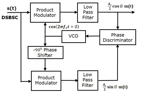
Costas loop consists of two product modulators with common input $s\left ( t \right )$, which is DSBSC wave. The other input for both product modulators is taken from Voltage Controlled Oscillator (VCO) with $-90^0$ phase shift to one of the product modulator as shown in figure.
We know that the equation of DSBSC wave is
$$s\left ( t \right )=A_c \cos\left ( 2 \pi f_ct \right )m\left ( t \right )$$
Let the output of VCO be
$$c_1\left ( t \right )=\cos\left ( 2 \pi f_ct + \phi\right )$$
This output of VCO is applied as the carrier input of the upper product modulator.
Hence, the output of the upper product modulator is
$$v_1\left ( t \right )=s\left ( t \right )c_1\left ( t \right )$$
Substitute, $s\left ( t \right )$ and $c_1\left ( t \right )$ values in the above equation.
$$\Rightarrow v_1\left ( t \right )=A_c \cos \left ( 2 \pi f_ct \right )m\left ( t \right ) \cos\left ( 2 \pi f_ct + \phi \right )$$
After simplifying, we will get $v_1\left ( t \right )$ as
$$v_1\left ( t \right )=\frac{A_c}{2} \cos \phi m\left ( t \right )+\frac{A_c}{2} \cos\left ( 4 \pi f_ct + \phi \right )m\left ( t \right )$$
This signal is applied as an input of the upper low pass filter. The output of this low pass filter is
$$v_{01}\left ( t \right )=\frac{A_c}{2} \cos \phi m\left ( t \right )$$
Therefore, the output of this low pass filter is the scaled version of the modulating signal.
The output of $-90^0$ phase shifter is
$$c_2\left ( t \right )=cos\left ( 2 \pi f_ct + \phi-90^0 \right )= \sin\left ( 2 \pi f_ct + \phi \right )$$
This signal is applied as the carrier input of the lower product modulator.
The output of the lower product modulator is
$$v_2\left ( t \right )=s\left ( t \right )c_2\left ( t \right )$$
Substitute, $s\left ( t \right )$ and $c_2\left ( t \right )$ values in the above equation.
$$\Rightarrow v_2\left ( t \right )=A_c \cos\left ( 2 \pi f_ct \right )m\left ( t \right ) \sin \left ( 2 \pi f_ct + \phi \right )$$
After simplifying, we will get $v_2\left ( t \right )$ as
$$v_2\left ( t \right )=\frac{A_c}{2} \sin \phi m\left ( t \right )+\frac{A_c}{2} \sin \left ( 4 \pi f_ct+ \phi \right )m\left ( t \right )$$
This signal is applied as an input of the lower low pass filter. The output of this low pass filter is
$$v_{02}\left ( t \right )=\frac{A_c}{2} \sin \phi m\left ( t \right )$$
The output of this Low pass filter has $-90^0$ phase difference with the output of the upper low pass filter.
The outputs of these two low pass filters are applied as inputs of the phase discriminator. Based on the phase difference between these two signals, the phase discriminator produces a DC control signal.
This signal is applied as an input of VCO to correct the phase error in VCO output. Therefore, the carrier signal (used for DSBSC modulation) and the locally generated signal (VCO output) are in phase.
Analog Communication - SSBSC Modulation
In the previous chapters, we have discussed DSBSC modulation and demodulation. The DSBSC modulated signal has two sidebands. Since, the two sidebands carry the same information, there is no need to transmit both sidebands. We can eliminate one sideband.
The process of suppressing one of the sidebands along with the carrier and transmitting a single sideband is called as Single Sideband Suppressed Carrier system or simply SSBSC. It is plotted as shown in the following figure.
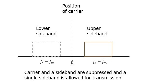
In the above figure, the carrier and the lower sideband are suppressed. Hence, the upper sideband is used for transmission. Similarly, we can suppress the carrier and the upper sideband while transmitting the lower sideband.
This SSBSC system, which transmits a single sideband has high power, as the power allotted for both the carrier and the other sideband is utilized in transmitting this Single Sideband.
Mathematical Expressions
Let us consider the same mathematical expressions for the modulating and the carrier signals as we have considered in the earlier chapters.
i.e., Modulating signal
$$m\left ( t \right )=A_m \cos\left ( 2 \pi f_mt \right )$$
Carrier signal
$$c\left ( t \right )=A_c \cos\left ( 2 \pi f_ct \right)$$
Mathematically, we can represent the equation of SSBSC wave as
$s\left ( t \right )=\frac{A_mA_c}{2} \cos\left [ 2 \pi\left ( f_c+f_m \right ) t\right ]$for the upper sideband
Or
$s\left ( t \right )=\frac{A_mA_c}{2} \cos\left [ 2 \pi\left ( f_c-f_m \right ) t\right ]$for the lower sideband
Bandwidth of SSBSC Wave
We know that the DSBSC modulated wave contains two sidebands and its bandwidth is $2f_m$. Since the SSBSC modulated wave contains only one sideband, its bandwidth is half of the bandwidth of DSBSC modulated wave.
i.e., Bandwidth of SSBSC modulated wave =$\frac{2f_m}{2}=f_m$
Therefore, the bandwidth of SSBSC modulated wave is $f_m$ and it is equal to the frequency of the modulating signal.
Power Calculations of SSBSC Wave
Consider the following equation of SSBSC modulated wave.
$s\left ( t \right )=\frac{A_mA_c}{2} \cos\left [ 2 \pi\left ( f_c+f_m \right ) t\right ]$for the upper sideband
Or
$s\left ( t \right )=\frac{A_mA_c}{2} \cos\left [ 2 \pi\left ( f_c-f_m \right ) t\right ]$for the lower sideband
Power of SSBSC wave is equal to the power of any one sideband frequency components.
$$P_t=P_{USB}=P_{LSB}$$
We know that the standard formula for power of cos signal is
$$P=\frac{{v_{rms}}^{2}}{R}=\frac{\left ( v_m/\sqrt{2} \right )^2}{R}$$
In this case, the power of the upper sideband is
$$P_{USB}=\frac{\left ( A_m A_c/2\sqrt{2} \right )^2}{R}=\frac{{A_{m}}^{2}{A_{c}}^{2}}{8R}$$
Similarly, we will get the lower sideband power same as that of the upper side band power.
$$P_{LSB}= \frac{{A_{m}}^{2}{A_{c}}^{2}}{8R}$$
Therefore, the power of SSBSC wave is
$$P_t=P_{USB}=P_{LSB}= \frac{{A_{m}}^{2}{A_{c}}^{2}}{8R}$$
Advantages
Bandwidth or spectrum space occupied is lesser than AM and DSBSC waves.
Transmission of more number of signals is allowed.
Power is saved.
High power signal can be transmitted.
Less amount of noise is present.
Signal fading is less likely to occur.
Disadvantages
The generation and detection of SSBSC wave is a complex process.
The quality of the signal gets affected unless the SSB transmitter and receiver have an excellent frequency stability.
Applications
For power saving requirements and low bandwidth requirements.
In land, air, and maritime mobile communications.
In point-to-point communications.
In radio communications.
In television, telemetry, and radar communications.
In military communications, such as amateur radio, etc.
Analog Communication - SSBSC Modulators
In this chapter, let us discuss about the modulators, which generate SSBSC wave. We can generate SSBSC wave using the following two methods.
- Frequency discrimination method
- Phase discrimination method
Frequency Discrimination Method
The following figure shows the block diagram of SSBSC modulator using frequency discrimination method.
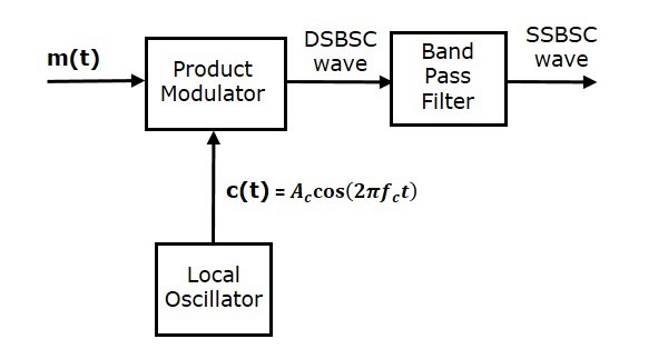
In this method, first we will generate DSBSC wave with the help of the product modulator. Then, apply this DSBSC wave as an input of band pass filter. This band pass filter produces an output, which is SSBSC wave.
Select the frequency range of band pass filter as the spectrum of the desired SSBSC wave. This means the band pass filter can be tuned to either upper sideband or lower sideband frequencies to get the respective SSBSC wave having upper sideband or lower sideband.
Phase Discrimination Method
The following figure shows the block diagram of SSBSC modulator using phase discrimination method.
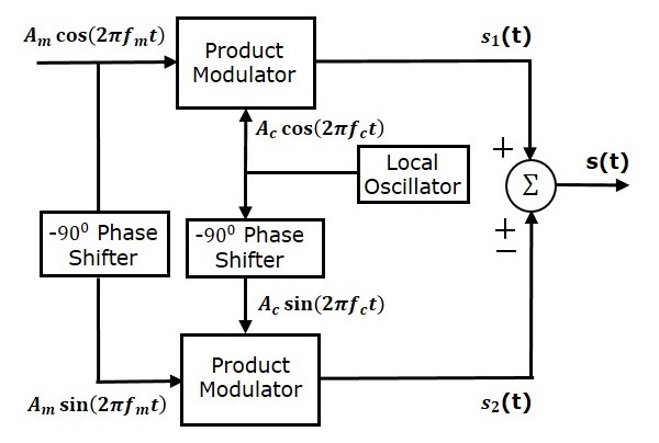
This block diagram consists of two product modulators, two $-90^0$ phase shifters, one local oscillator and one summer block. The product modulator produces an output, which is the product of two inputs. The $-90^0$ phase shifter produces an output, which has a phase lag of $-90^0$ with respect to the input.
The local oscillator is used to generate the carrier signal. Summer block produces an output, which is either the sum of two inputs or the difference of two inputs based on the polarity of inputs.
The modulating signal $A_m \cos\left ( 2 \pi f_mt \right )$ and the carrier signal $A_c \cos\left ( 2 \pi f_ct \right )$ are directly applied as inputs to the upper product modulator. So, the upper product modulator produces an output, which is the product of these two inputs.
The output of upper product modulator is
$$s_1\left ( t \right )=A_mA_c \cos \left ( 2 \pi f_mt \right ) \cos\left ( 2 \pi f_ct \right )$$
$$ \Rightarrow s_1\left ( t \right )=\frac{A_mA_c}{2} \left \{ \cos \left [ 2 \pi\left ( f_c+f_m \right )t \right ]+ \cos\left [ 2 \pi\left ( f_c-f_m \right )t \right ] \right \}$$
The modulating signal $A_m \cos\left ( 2 \pi f_mt \right )$ and the carrier signal $A_c \cos\left ( 2 \pi f_ct \right )$ are phase shifted by $-90^0$ before applying as inputs to the lower product modulator. So, the lower product modulator produces an output, which is the product of these two inputs.
The output of lower product modulator is
$$s_2\left ( t \right )=A_mA_c \cos\left ( 2 \pi f_mt-90^0 \right ) \cos\left (2 \pi f_ct-90^0 \right )$$
$\Rightarrow s_2\left ( t \right )=A_mA_c \sin \left ( 2 \pi f_mt \right )\sin \left ( 2 \pi f_ct \right )$
$\Rightarrow s_2\left ( t \right )=\frac{A_mA_c}{2} \left \{ \cos \left [ 2 \pi\left ( f_c-f_m \right )t \right ]- \cos\left [ 2 \pi\left ( f_c+f_m \right )t \right ] \right \}$
Add $s_1\left ( t \right )$ and $s_2\left ( t \right )$ in order to get the SSBSC modulated wave $s\left ( t \right )$ having a lower sideband.
$s\left ( t \right )=\frac{A_mA_c}{2}\left \{ \cos\left [ 2 \pi\left ( f_c+f_m \right )t \right ]+\cos\left [ 2 \pi\left ( f_c-f_m \right )t \right ] \right \}+$
$\frac{A_mA_c}{2}\left \{ \cos\left [ 2 \pi\left ( f_c-f_m \right )t \right ]-\cos\left [ 2 \pi\left ( f_c+f_m \right )t \right ] \right \}$
$\Rightarrow s\left ( t \right )=A_mA_c \cos \left [ 2 \pi\left ( f_c-f_m \right )t \right ]$
Subtract $s_2\left ( t \right )$ from $s_1\left ( t \right )$ in order to get the SSBSC modulated wave $s\left ( t \right )$ having a upper sideband.
$s\left ( t \right )=\frac{A_mA_c}{2}\left \{ \cos\left [ 2 \pi\left ( f_c+f_m \right )t \right ]+\cos\left [ 2 \pi\left ( f_c-f_m \right )t \right ] \right \}-$
$\frac{A_mA_c}{2}\left \{ \cos\left [ 2 \pi\left ( f_c-f_m \right )t \right ]-\cos\left [ 2 \pi\left ( f_c+f_m \right )t \right ] \right \}$
$\Rightarrow s\left ( t \right )=A_mA_c \cos \left [ 2 \pi\left ( f_c+f_m \right )t \right ]$
Hence, by properly choosing the polarities of inputs at summer block, we will get SSBSC wave having a upper sideband or a lower sideband.
SSBSC Demodulator
The process of extracting an original message signal from SSBSC wave is known as detection or demodulation of SSBSC. Coherent detector is used for demodulating SSBSC wave.
Coherent Detector
Here, the same carrier signal (which is used for generating SSBSC wave) is used to detect the message signal. Hence, this process of detection is called as coherent or synchronous detection. Following is the block diagram of coherent detector.
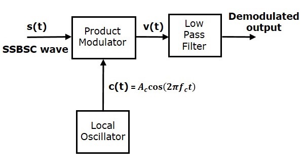
In this process, the message signal can be extracted from SSBSC wave by multiplying it with a carrier, having the same frequency and the phase of the carrier used in SSBSC modulation. The resulting signal is then passed through a Low Pass Filter. The output of this filter is the desired message signal.
Consider the following SSBSC wave having a lower sideband.
$$s\left ( t \right )=\frac{A_mA_c}{2} \cos\left [ 2 \pi\left ( f_c-f_m \right )t \right ]$$
The output of the local oscillator is
$$c\left ( t \right )=A_c \cos\left ( 2 \pi f_ct \right )$$
From the figure, we can write the output of product modulator as
$$v\left ( t \right )=s\left ( t \right )c\left ( t \right )$$
Substitute $s\left ( t \right )$ and $c\left ( t \right )$ values in the above equation.
$$v\left ( t \right )=\frac{A_mA_c}{2} \cos \left [ 2 \pi \left ( f_c-f_m \right )t \right ] A_c \cos \left ( 2 \pi f_ct \right )$$
$=\frac{A_m{A_{c}}^{2}}{2} \cos\left [ 2 \pi\left ( f_c -f_m \right )t \right ] \cos\left ( 2 \pi f_ct \right )$
$=\frac{A_m{A_{c}}^{2}}{4}\left \{ \cos\left [ 2 \pi\left ( 2f_c-fm \right ) \right ]+ \cos\left ( 2 \pi f_m \right )t \right \}$
$v\left ( t \right )=\frac{A_m{A_{c}}^{2}}{4} \cos\left ( 2 \pi f_mt \right )+\frac{A_m{A_{c}}^{2}}{4} \cos\left [ 2 \pi \left ( 2f_c-f_m \right )t \right ]$
In the above equation, the first term is the scaled version of the message signal. It can be extracted by passing the above signal through a low pass filter.
Therefore, the output of low pass filter is
$$v_0\left ( t \right )=\frac{A_m{A_{c}}^{2}}{4} \cos\left ( 2 \pi f_mt \right )$$
Here, the scaling factor is $\frac{{A_{c}}^{2}}{4}$.
We can use the same block diagram for demodulating SSBSC wave having an upper sideband. Consider the following SSBSC wave having an upper sideband.
$$s\left ( t \right )=\frac{A_mA_c}{2} \cos\left [ 2 \pi \left ( f_c+f_m \right )t \right ]$$
The output of the local oscillator is
$$c\left ( t \right )=A_c \cos\left ( 2 \pi f_ct \right )$$
We can write the output of the product modulator as
$$v\left ( t \right )=s\left ( t \right )c\left ( t \right )$$
Substitute $s\left ( t \right )$ and $c\left ( t \right )$ values in the above equation.
$$\Rightarrow v\left ( t \right )=\frac{A_mA_c}{2} \cos\left [ 2 \pi\left ( f_c+f_m \right )t \right ]A_c \cos\left ( 2 \pi f_ct \right )$$
$=\frac{A_m{A_{c}}^{2}}{2} \cos\left [ 2 \pi\left ( f_c+f_m \right )t \right ] \cos\left ( 2 \pi f_ct \right )$
$=\frac{A_m{A_{c}}^{2}}{4} \left \{ \cos\left [ 2 \pi\left ( 2f_c+f_m \right )t \right ]+ \cos\left ( 2 \pi f_mt \right ) \right \}$
$v\left ( t \right )=\frac{A_m{A_{c}}^{2}}{4} \cos\left ( 2 \pi f_mt \right )+\frac{A_m{A_{c}}^{2}}{4} \cos \left [ 2 \pi\left ( 2f_c+f_m \right )t \right ]$
In the above equation, the first term is the scaled version of the message signal. It can be extracted by passing the above signal through a low pass filter.
Therefore, the output of the low pass filter is
$$v_0\left ( t \right )=\frac{A_m{A_{c}}^{2}}{4} \cos\left ( 2 \pi f_mt \right )$$
Here too the scaling factor is $\frac{{A_{c}}^{2}}{4}$.
Therefore, we get the same demodulated output in both the cases by using coherent detector.
Analog Communication - VSBSC Modulation
In the previous chapters, we have discussed SSBSC modulation and demodulation. SSBSC modulated signal has only one sideband frequency. Theoretically, we can get one sideband frequency component completely by using an ideal band pass filter. However, practically we may not get the entire sideband frequency component. Due to this, some information gets lost.
To avoid this loss, a technique is chosen, which is a compromise between DSBSC and SSBSC. This technique is known as Vestigial Side Band Suppressed Carrier (VSBSC) technique. The word vestige means a part from which, the name is derived.
VSBSC Modulation is the process, where a part of the signal called as vestige is modulated along with one sideband. The frequency spectrum of VSBSC wave is shown in the following figure.
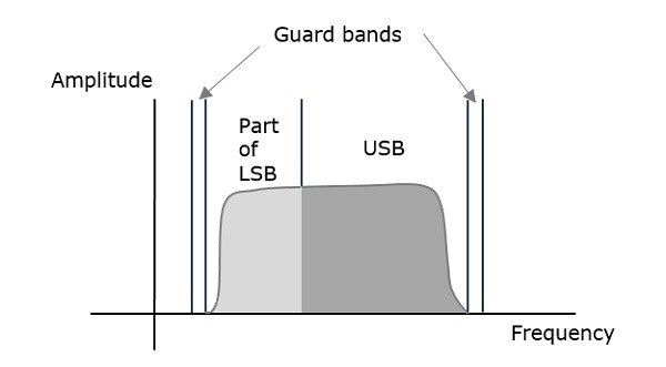
Along with the upper sideband, a part of the lower sideband is also being transmitted in this technique. Similarly, we can transmit the lower sideband along with a part of the upper sideband. A guard band of very small width is laid on either side of VSB in order to avoid the interferences. VSB modulation is mostly used in television transmissions.
Bandwidth of VSBSC Modulation
We know that the bandwidth of SSBSC modulated wave is $f_m$. Since the VSBSC modulated wave contains the frequency components of one side band along with the vestige of other sideband, the bandwidth of it will be the sum of the bandwidth of SSBSC modulated wave and vestige frequency $f_v$.
i.e., Bandwidth of VSBSC Modulated Wave = $f_m + f_v$
Advantages
Following are the advantages of VSBSC modulation.
Highly efficient.
Reduction in bandwidth when compared to AM and DSBSC waves.
Filter design is easy, since high accuracy is not needed.
The transmission of low frequency components is possible, without any difficulty.
Possesses good phase characteristics.
Disadvantages
Following are the disadvantages of VSBSC modulation.
Bandwidth is more when compared to SSBSC wave.
Demodulation is complex.
Applications
The most prominent and standard application of VSBSC is for the transmission of television signals. Also, this is the most convenient and efficient technique when bandwidth usage is considered.
Now, let us discuss about the modulator which generates VSBSC wave and the demodulator which demodulates VSBSC wave one by one.
Generation of VSBSC
Generation of VSBSC wave is similar to the generation of SSBSC wave. The VSBSC modulator is shown in the following figure.
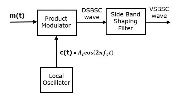
In this method, first we will generate DSBSC wave with the help of the product modulator. Then, apply this DSBSC wave as an input of sideband shaping filter. This filter produces an output, which is VSBSC wave.
The modulating signal $m\left ( t \right )$ and carrier signal $A_c \cos \left ( 2 \pi f_ct \right )$ are applied as inputs to the product modulator. Hence, the product modulator produces an output, which is the product of these two inputs.
Therefore, the output of the product modulator is
$$p\left ( t \right )=A_c \cos\left ( 2 \pi f_ct \right )m\left ( t \right )$$
Apply Fourier transform on both sides
$$P\left ( f \right )=\frac{A_c}{2}\left [ M\left ( f-f_c \right )+M\left ( f+f_c \right ) \right ]$$
The above equation represents the equation of DSBSC frequency spectrum.
Let the transfer function of the sideband shaping filter be $H\left ( f \right )$. This filter has the input $p\left ( t \right )$ and the output is VSBSC modulated wave $s\left ( t \right )$. The Fourier transforms of $p\left ( t \right )$ and $s\left ( t \right )$ are $P\left ( t \right )$ and $S\left ( t \right )$ respectively.
Mathematically, we can write $S\left ( f \right )$ as
$$S\left ( t \right )=P\left ( f \right )H\left ( f \right )$$
Substitute $P\left ( f \right )$ value in the above equation.
$$S\left ( f \right )=\frac{A_c}{2}\left [ M\left ( f-f_c \right )+M\left ( f+f_c \right ) \right ]H\left ( f \right )$$
The above equation represents the equation of VSBSC frequency spectrum.
Demodulation of VSBSC
Demodulation of VSBSC wave is similar to the demodulation of SSBSC wave. Here, the same carrier signal (which is used for generating VSBSC wave) is used to detect the message signal. Hence, this process of detection is called as coherent or synchronous detection. The VSBSC demodulator is shown in the following figure.
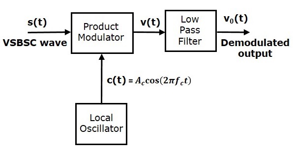
In this process, the message signal can be extracted from VSBSC wave by multiplying it with a carrier, which is having the same frequency and the phase of the carrier used in VSBSC modulation. The resulting signal is then passed through a Low Pass Filter. The output of this filter is the desired message signal.
Let the VSBSC wave be $s\left ( t \right )$ and the carrier signal is $A_c \cos \left ( 2 \pi f_ct \right )$.
From the figure, we can write the output of the product modulator as
$$v\left ( t \right )= A_c \cos\left ( 2 \pi f_ct \right )s\left ( t \right )$$
Apply Fourier transform on both sides
$$V\left ( f \right )= \frac{A_c}{2}\left [ S\left ( f-f_c \right )+S\left ( f+f_c \right ) \right ]$$
We know that$S\left ( f \right )=\frac{A_c}{2}\left [ M\left ( f-f_c \right ) + M\left ( f+f_c \right )\right ]H\left ( f \right )$
From the above equation, let us find $S\left ( f-f_c \right )$ and $S\left ( f+f_c \right )$.
$$S\left ( f-f_c \right )=\frac{A_c}{2}\left [ M\left ( f-f_c-f_c \right ) + M\left ( f-f_c+f_c \right )\right ]H\left ( f-f_c \right )$$
$\Rightarrow S\left ( f-f_c \right )=\frac{A_c}{2}\left [ M\left ( f-2f_c \right )+M\left ( f \right ) \right ] H\left ( f-f_c \right )$
$$S\left ( f+f_c \right )=\frac{A_c}{2}\left [ M\left ( f+f_c-f_c \right ) +M\left ( f+f_c+f_c \right )\right ] H\left ( f+f_c \right )$$
$\Rightarrow S\left ( f+f_c \right )=\frac{A_c}{2}\left [ M \left ( f \right )+M \left (f+2f_c \right ) \right ] H \left ( f+f_c \right )$
Substitute, $S\left ( f-f_c \right )$ and $S\left ( f+f_c \right )$ values in $V\left ( f \right )$.
$V(f) = \frac{A_c}{2}[\frac{A_c}{2}[M(f-2f_c)+M(f)]H(f-f_c)+$
$\frac{A_c}{2}[M(f)+M(f+2f_c)]H(f+f_c)]$
$\Rightarrow V\left ( f \right )=\frac{{A_{c}}^{2}}{4} M\left ( f \right )\left [ H\left ( f-f_c \right )+H \left ( f+f_c \right ) \right ]$
$+ \frac{{A_{c}}^{2}}{4}\left [ M\left ( f-2f_c \right )H\left ( f-f_c \right )+M\left ( f+2f_c \right )H\left ( f+f_c \right ) \right ]$
In the above equation, the first term represents the scaled version of the desired message signal frequency spectrum. It can be extracted by passing the above signal through a low pass filter.
$$V_0\left ( f \right )=\frac{{A_{c}}^{2}}{4} M\left ( f \right )\left [ H\left ( f-f_c \right )+H\left ( f+f_c \right ) \right ]$$
Analog Communication - Angle Modulation
The other type of modulation in continuous-wave modulation is Angle Modulation. Angle Modulation is the process in which the frequency or the phase of the carrier signal varies according to the message signal.
The standard equation of the angle modulated wave is
$$s\left ( t \right )=A_c \cos \theta _i\left ( t \right )$$
Where,
$A_c$ is the amplitude of the modulated wave, which is the same as the amplitude of the carrier signal
$\theta _i\left ( t \right )$ is the angle of the modulated wave
Angle modulation is further divided into frequency modulation and phase modulation.
Frequency Modulation is the process of varying the frequency of the carrier signal linearly with the message signal.
Phase Modulation is the process of varying the phase of the carrier signal linearly with the message signal.
Now, let us discuss these in detail.
Frequency Modulation
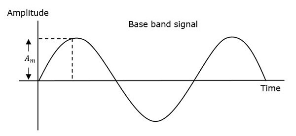
In amplitude modulation, the amplitude of the carrier signal varies. Whereas, in Frequency Modulation (FM), the frequency of the carrier signal varies in accordance with the instantaneous amplitude of the modulating signal.
Hence, in frequency modulation, the amplitude and the phase of the carrier signal remains constant. This can be better understood by observing the following figures.

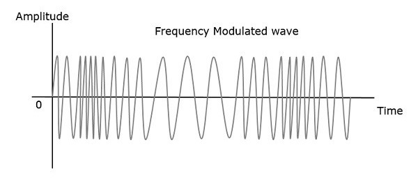
The frequency of the modulated wave increases, when the amplitude of the modulating or message signal increases. Similarly, the frequency of the modulated wave decreases, when the amplitude of the modulating signal decreases. Note that, the frequency of the modulated wave remains constant and it is equal to the frequency of the carrier signal, when the amplitude of the modulating signal is zero.
Mathematical Representation
The equation for instantaneous frequency $f_i$ in FM modulation is
$$f_i=f_c+k_fm\left ( t \right )$$
Where,
$f_c$ is the carrier frequency
$k_t$ is the frequency sensitivity
$m\left ( t \right )$ is the message signal
We know the relationship between angular frequency $\omega_i$ and angle $\theta _i\left ( t \right )$ as
$$\omega_i=\frac{d\theta _i\left ( t \right )}{dt}$$
$\Rightarrow 2 \pi f_i=\frac{d\theta _i\left ( t \right )}{dt}$
$\Rightarrow \theta _i\left ( t \right )= 2\pi\int f_i dt$
Substitute, $f_i$ value in the above equation.
$$\theta _i\left ( t \right )=2 \pi\int \left ( f_c+k_f m\left ( t \right ) \right )dt$$
$\Rightarrow \theta _i\left ( t \right )=2 \pi f_ct+2 \pi k_f\int m\left ( t \right )dt$
Substitute, $\theta _i\left ( t \right )$ value in the standard equation of angle modulated wave.
$$s\left ( t \right )=A_c \cos\left ( 2 \pi f_ct + 2 \pi k_f \int m\left ( t \right )dt \right )$$
This is the equation of FM wave.
If the modulating signal is $m\left ( t \right )= A_m \cos \left ( 2 \pi f_mt \right )$, then the equation of FM wave will be
$$s\left ( t \right )=A_c \cos\left ( 2 \pi f_ct + \beta \sin \left ( 2 \pi f_mt \right ) \right )$$
Where,
$\beta$ = modulation index $=\frac{\Delta f}{f_m}=\frac{k_fA_m}{f_m}$
The difference between FM modulated frequency (instantaneous frequency) and normal carrier frequency is termed as Frequency Deviation. It is denoted by $\Delta f$, which is equal to the product of $k_f$ and $A_m$.
FM can be divided into Narrowband FM and Wideband FM based on the values of modulation index $\beta$.
Narrowband FM
Following are the features of Narrowband FM.
This frequency modulation has a small bandwidth when compared to wideband FM.
The modulation index $\beta$ is small, i.e., less than 1.
Its spectrum consists of the carrier, the upper sideband and the lower sideband.
This is used in mobile communications such as police wireless, ambulances, taxicabs, etc.
Wideband FM
Following are the features of Wideband FM.
This frequency modulation has infinite bandwidth.
The modulation index $\beta$ is large, i.e., higher than 1.
Its spectrum consists of a carrier and infinite number of sidebands, which are located around it.
This is used in entertainment, broadcasting applications such as FM radio, TV, etc.
Phase Modulation
In frequency modulation, the frequency of the carrier varies. Whereas, in Phase Modulation (PM), the phase of the carrier signal varies in accordance with the instantaneous amplitude of the modulating signal.
So, in phase modulation, the amplitude and the frequency of the carrier signal remains constant. This can be better understood by observing the following figures.

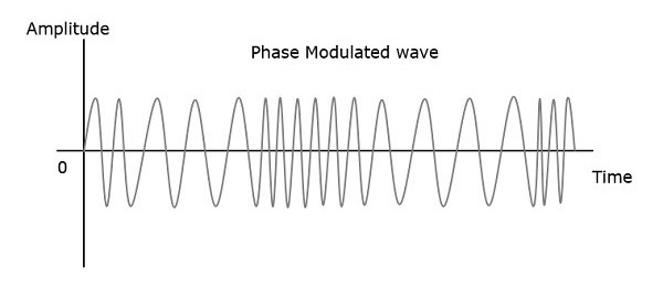
The phase of the modulated wave has got infinite points, where the phase shift in a wave can take place. The instantaneous amplitude of the modulating signal changes the phase of the carrier signal. When the amplitude is positive, the phase changes in one direction and if the amplitude is negative, the phase changes in the opposite direction.
Mathematical Representation
The equation for instantaneous phase $\phi_i$ in phase modulation is
$$\phi _i=k_p m\left ( t \right )$$
Where,
$k_p$ is the phase sensitivity
$m\left ( t \right )$ is the message signal
The standard equation of angle modulated wave is
$$s\left ( t \right )=A_c \cos \left ( 2 \pi f_ct+\phi_i \right )$$
Substitute, $\phi_i$ value in the above equation.
$$s\left ( t \right )=A_c \cos \left ( 2 \pi f_ct+k_p m \left ( t \right )\right )$$
This is the equation of PM wave.
If the modulating signal, $m\left ( t \right )=A_m \cos \left ( 2 \pi f_mt \right ) $, then the equation of PM wave will be
$$s\left ( t \right )=A_c \cos\left (2 \pi f_ct+\beta \cos\left ( 2 \pi f_mt \right ) \right )$$
Where,
$\beta$ = modulation index = $\Delta \phi=k_pA_m$
$\Delta \phi$ is phase deviation
Phase modulation is used in mobile communication systems, while frequency modulation is used mainly for FM broadcasting.
Numerical Problems 2
In the previous chapter, we have discussed the parameters used in Angle modulation. Each parameter has its own formula. By using those formulas, we can find the respective parameter values. In this chapter, let us solve a few problems based on the concept of Frequency Modulation.
Problem 1
A sinusoidal modulating waveform of amplitude 5 V and a frequency of 2 KHz is applied to FM generator, which has a frequency sensitivity of 40 Hz/volt. Calculate the frequency deviation, modulation index, and bandwidth.
Solution
Given, the amplitude of modulating signal, $A_m=5V$
Frequency of modulating signal, $f_m=2 KHz$
Frequency sensitivity, $k_f=40 Hz/volt$
We know the formula for Frequency deviation as
$$\Delta f=k_f A_m$$
Substitute $k_f$ and $A_m$ values in the above formula.
$$\Delta f=40 \times 5=200Hz$$
Therefore, frequency deviation, $\Delta f$ is $200Hz$
The formula for modulation index is
$$\beta = \frac{\Delta f}{f_m}$$
Substitute $\Delta f$ and $f_m$ values in the above formula.
$$\beta=\frac{200}{2 \times 1000}=0.1$$
Here, the value of modulation index, $\beta$ is 0.1, which is less than one. Hence, it is Narrow Band FM.
The formula for Bandwidth of Narrow Band FM is the same as that of AM wave.
$$BW=2f_m$$
Substitute $f_m$ value in the above formula.
$$BW=2 \times 2K=4KHz$$
Therefore, the bandwidth of Narrow Band FM wave is $4 KHz$.
Problem 2
An FM wave is given by $s\left ( t \right )=20 \cos\left ( 8 \pi \times10^6t+9 \sin\left ( 2 \pi \times 10^3 t \right ) \right )$. Calculate the frequency deviation, bandwidth, and power of FM wave.
Solution
Given, the equation of an FM wave as
$$s\left ( t \right )=20 \cos\left ( 8 \pi \times10^6t+9 \sin\left ( 2 \pi \times 10^3 t \right ) \right )$$
We know the standard equation of an FM wave as
$$s\left ( t \right )=A_c \cos\left ( 2 \pi f_ct + \beta \sin \left ( 2 \pi f_mt \right ) \right )$$
We will get the following values by comparing the above two equations.
Amplitude of the carrier signal, $A_c=20V$
Frequency of the carrier signal, $f_c=4 \times 10^6 Hz=4 MHz$
Frequency of the message signal, $f_m=1 \times 10^3 Hz = 1KHz$
Modulation index, $\beta=9$
Here, the value of modulation index is greater than one. Hence, it is Wide Band FM.
We know the formula for modulation index as
$$\beta=\frac {\Delta f}{f_m}$$
Rearrange the above equation as follows.
$$\Delta=\beta f_m$$
Substitute $\beta$ and $f_m$ values in the above equation.
$$\Delta=9 \times 1K =9 KHz$$
Therefore, frequency deviation, $\Delta f$ is $9 KHz$.
The formula for Bandwidth of Wide Band FM wave is
$$BW=2\left ( \beta +1 \right )f_m$$
Substitute $\beta$ and $f_m$ values in the above formula.
$$BW=2\left ( 9 +1 \right )1K=20KHz$$
Therefore, the bandwidth of Wide Band FM wave is $20 KHz$
Formula for power of FM wave is
$$P_c= \frac{{A_{c}}^{2}}{2R}$$
Assume, $R=1\Omega$ and substitute $A_c$ value in the above equation.
$$P=\frac{\left ( 20 \right )^2}{2\left ( 1 \right )}=200W$$
Therefore, the power of FM wave is $200$ watts.
Analog Communication - FM Modulators
In this chapter, let us discuss about the modulators which generate NBFM and WBFM waves. First, let us discuss about the generation of NBFM.
Generation of NBFM
We know that the standard equation of FM wave is
$$s\left ( t \right )=A_c \cos\left ( 2 \pi f_ct+2 \pi k_f\int m\left ( t \right ) dt\right )$$
$\Rightarrow s\left ( t \right )=A_c \cos\left ( 2 \pi f_ct \right ) \cos\left ( 2 \pi k_f\int m\left ( t \right )dt \right )-$
$A_c \sin\left ( 2 \pi f_ct \right ) \sin\left ( 2 \pi k_f\int m\left ( t \right )dt \right )$
For NBFM,
$$\left | 2 \pi k_f\int m\left ( t \right )dt \right |
We know that $\cos \theta \approx 1$ and $\sin \theta \approx 1$ when $\theta$ is very small.
By using the above relations, we will get the NBFM equation as
$$s\left ( t \right )=A_c \cos\left ( 2 \pi f_ct \right )-A_c \sin\left ( 2 \pi f_ct \right )2 \pi k_f\int m\left ( t \right )dt$$
The block diagram of NBFM modulator is shown in the following figure.
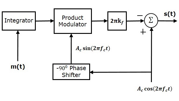
Here, the integrator is used to integrate the modulating signal $m\left (t \right )$. The carrier signal $A_c \cos \left ( 2 \pi f_ct \right )$ is the phase shifted by $-90^0$ to get $A_c \sin \left ( 2 \pi f_ct \right )$ with the help of $-90^0$ phase shifter. The product modulator has two inputs $\int m\left ( t \right )dt$ and $A_c \sin \left ( 2 \pi f_ct \right )$. It produces an output, which is the product of these two inputs.
This is further multiplied with $2 \pi k_f$ by placing a block $2 \pi k_f$ in the forward path. The summer block has two inputs, which are nothing but the two terms of NBFM equation. Positive and negative signs are assigned for the carrier signal and the other term at the input of the summer block. Finally, the summer block produces NBFM wave.
Generation of WBFM
The following two methods generate WBFM wave.
- Direct method
- Indirect method
Direct Method
This method is called as the Direct Method because we are generating a wide band FM wave directly. In this method, Voltage Controlled Oscillator (VCO) is used to generate WBFM. VCO produces an output signal, whose frequency is proportional to the input signal voltage. This is similar to the definition of FM wave. The block diagram of the generation of WBFM wave is shown in the following figure.
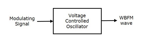
Here, the modulating signal $m\left (t \right )$ is applied as an input of Voltage Controlled Oscillator (VCO). VCO produces an output, which is nothing but the WBFM.
$$f_i \: \alpha \: m\left ( t \right )$$
$$\Rightarrow f_i=f_c+k_fm\left ( t \right )$$
Where,
$f_i$ is the instantaneous frequency of WBFM wave.
Indirect Method
This method is called as Indirect Method because we are generating a wide band FM wave indirectly. This means, first we will generate NBFM wave and then with the help of frequency multipliers we will get WBFM wave. The block diagram of generation of WBFM wave is shown in the following figure.
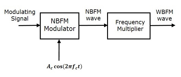
This block diagram contains mainly two stages. In the first stage, the NBFM wave will be generated using NBFM modulator. We have seen the block diagram of NBFM modulator at the beginning of this chapter. We know that the modulation index of NBFM wave is less than one. Hence, in order to get the required modulation index (greater than one) of FM wave, choose the frequency multiplier value properly.
Frequency multiplier is a non-linear device, which produces an output signal whose frequency is n times the input signal frequency. Where, n is the multiplication factor.
If NBFM wave whose modulation index $\beta$ is less than 1 is applied as the input of frequency multiplier, then the frequency multiplier produces an output signal, whose modulation index is n times $\beta$ and the frequency also n times the frequency of WBFM wave.
Sometimes, we may require multiple stages of frequency multiplier and mixers in order to increase the frequency deviation and modulation index of FM wave.
Analog Communication - FM Demodulators
In this chapter, let us discuss about the demodulators which demodulate the FM wave. The following two methods demodulate FM wave.
- Frequency discrimination method
- Phase discrimination method
Frequency Discrimination Method
We know that the equation of FM wave is
$$s\left ( t \right ) =A_c \cos \left ( 2 \pi f_ct+2 \pi k_f \int m\left ( t \right )dt \right )$$
Differentiate the above equation with respect to 't'.
$$\frac{ds\left ( t \right )}{dt}= -A_c\left ( 2 \pi f_c+2 \pi k_fm\left ( t \right ) \right ) \sin\left ( 2 \pi f_ct+2 \pi k_f\int m\left ( t \right )dt \right )$$
We can write, $-\sin \theta$ as $\sin \left ( \theta -180^0 \right )$.
$$\Rightarrow \frac{ds(t)}{dt}=A_c\left ( 2 \pi f_c+2 \pi k_fm\left ( t \right ) \right )\sin\left ( 2 \pi f_ct+2 \pi k_f \int m\left ( t \right )dt-180^0 \right )$$
$$\Rightarrow \frac{ds(t)}{dt}=A_c\left ( 2 \pi f_c \right )\left [ 1+\left ( \frac{k_f}{k_c} \right )m\left ( t \right ) \right ] \sin\left ( 2 \pi f_ct+2 \pi k_f\int m\left ( t \right )dt-180^0 \right )$$
In the above equation, the amplitude term resembles the envelope of AM wave and the angle term resembles the angle of FM wave. Here, our requirement is the modulating signal $m\left ( t \right )$. Hence, we can recover it from the envelope of AM wave.
The following figure shows the block diagram of FM demodulator using frequency discrimination method.
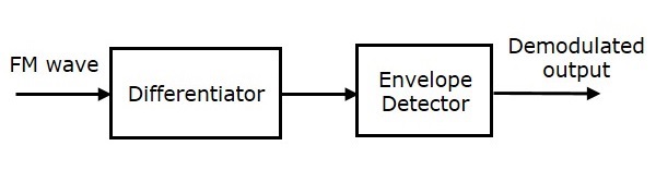
This block diagram consists of the differentiator and the envelope detector. Differentiator is used to convert the FM wave into a combination of AM wave and FM wave. This means, it converts the frequency variations of FM wave into the corresponding voltage (amplitude) variations of AM wave. We know the operation of the envelope detector. It produces the demodulated output of AM wave, which is nothing but the modulating signal.
Phase Discrimination Method
The following figure shows the block diagram of FM demodulator using phase discrimination method.
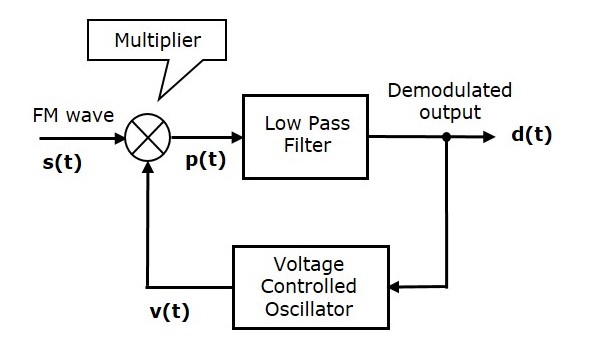
This block diagram consists of the multiplier, the low pass filter, and the Voltage Controlled Oscillator (VCO). VCO produces an output signal $v \left ( t \right )$, whose frequency is proportional to the input signal voltage $d \left ( t \right )$. Initially, when the signal $d \left ( t \right )$ is zero, adjust the VCO to produce an output signal $v \left ( t \right )$, having a carrier frequency and $-90^0$ phase shift with respect to the carrier signal.
FM wave $s \left ( t \right )$ and the VCO output $v \left ( t \right )$ are applied as inputs of the multiplier. The multiplier produces an output, having a high frequency component and a low frequency component. Low pass filter eliminates the high frequency component and produces only the low frequency component as its output.
This low frequency component contains only the term-related phase difference. Hence, we get the modulating signal $m \left ( t \right )$ from this output of the low pass filter.
Analog Communication - Multiplexing
Multiplexing is the process of combining multiple signals into one signal, over a shared medium. If the analog signals are multiplexed, then it is called as analog multiplexing. Similarly, if the digital signals are multiplexed, then it is called as digital multiplexing.
Multiplexing was first developed in telephony. A number of signals were combined to send through a single cable. The process of multiplexing divides a communication channel into several number of logical channels, allotting each one for a different message signal or a data stream to be transferred. The device that does multiplexing can be called as Multiplexer or MUX.
The reverse process, i.e., extracting the number of channels from one, which is done at the receiver is called as de-multiplexing. The device that does de-multiplexing can be called as de-multiplexer or DEMUX.
The following figures illustrates the concept of MUX and DEMUX. Their primary use is in the field of communications.
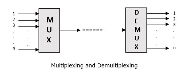
Types of Multiplexers
There are mainly two types of multiplexers, namely analog and digital. They are further divided into Frequency Division Multiplexing (FDM), Wavelength Division Multiplexing (WDM), and Time Division Multiplexing (TDM). The following figure gives a detailed idea about this classification.
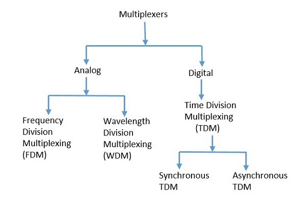
There are many types of multiplexing techniques. Out of which, we have the main types with general classification, mentioned in the above figure. Let us take a look at them individually.
Analog Multiplexing
The signals used in analog multiplexing techniques are analog in nature. The analog signals are multiplexed according to their frequency (FDM) or wavelength (WDM).
Frequency Division Multiplexing
In analog multiplexing, the most used technique is Frequency Division Multiplexing (FDM). This technique uses various frequencies to combine streams of data, for sending them on a communication medium, as a single signal.
Example − A traditional television transmitter, which sends a number of channels through a single cable uses FDM.
Wavelength Division Multiplexing
Wavelength Division multiplexing (WDM) is an analog technique, in which many data streams of different wavelengths are transmitted in the light spectrum. If the wavelength increases, the frequency of the signal decreases. A prism, which can turn different wavelengths into a single line, can be used at the output of MUX and input of DEMUX.
Example − Optical fiber communications use WDM technique, to merge different wavelengths into a single light for communication.
Digital Multiplexing
The term digital represents the discrete bits of information. Hence, the available data is in the form of frames or packets, which are discrete.
Time Division Multiplexing
In Time Division Multiplexing (TDM), the time frame is divided into slots. This technique is used to transmit a signal over a single communication channel, by allotting one slot for each message.
Time Division Multiplexing (TDM) can be classified into Synchronous TDM and Asynchronous TDM.
Synchronous TDM
In Synchronous TDM, the input is connected to a frame. If there are n number of connections, then the frame is divided into n time slots. One slot is allocated for each input line.
In this technique, the sampling rate is common for all signals and hence the same clock input is given. The MUX allocates the same slot to each device at all times.
Asynchronous TDM
In Asynchronous TDM, the sampling rate is different for each of the signals and a common clock is not required. If the allotted device for a time slot transmits nothing and sits idle, then that slot can be allotted to another device, unlike synchronous
This type of TDM is used in Asynchronous transfer mode networks.
De-Multiplexer
De-multiplexers are used to connect a single source to multiple destinations. This process is the reverse process of multiplexing. As mentioned previously, it is used mostly at the receivers. DEMUX has many applications. It is used in receivers in the communication systems. It is used in arithmetic and logical unit in computers to supply power and to pass on communication, etc.
De-multiplexers are used as serial to parallel converters. The serial data is given as input to DEMUX at regular interval and a counter is attached to it to control the output of the de-multiplexer.
Both the multiplexers and de-multiplexers play an important role in communication systems, both at the transmitter and the receiver sections.
Analog Communication - Noise
In any communication system, during the transmission of the signal or while receiving the signal, some unwanted signal gets introduced into the communication, making it unpleasant for the receiver, and questioning the quality of the communication. Such a disturbance is called as Noise.
What is Noise?
Noise is an unwanted signal, which interferes with the original message signal and corrupts the parameters of the message signal. This alteration in the communication process, leads to the message getting altered. It most likely enters at the channel or the receiver.
The noise signal can be understood by taking a look at the following figure.
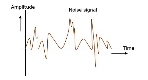
Hence, it is understood that the noise is some signal which has no pattern and no constant frequency or amplitude. It is quite random and unpredictable. Measures are usually taken to reduce it, though it cant be completely eliminated.
Most common examples of noise are −
Hiss sound in radio receivers
Buzz sound amidst of telephone conversations
Flicker in television receivers, etc
Types of Noise
The classification of noise is done depending on the type of the source, the effect it shows or the relation it has with the receiver, etc.
There are two main ways in which noise is produced. One is through some external source while the other is created by an internal source, within the receiver section.
External Source
This noise is produced by the external sources, which may occur in the medium or channel of communication usually. This noise cannot be completely eliminated. The best way is to avoid the noise from affecting the signal.
Examples
Most common examples of this type of noise are
Atmospheric noise (due to irregularities in the atmosphere).
Extra-terrestrial noise, such as solar noise and cosmic noise.
Industrial noise.
Internal Source
This noise is produced by the receiver components while functioning. The components in the circuits, due to continuous functioning, may produce few types of noise. This noise is quantifiable. A proper receiver design may lower the effect of this internal noise.
Examples
Most common examples of this type of noise are
Thermal agitation noise (Johnson noise or Electrical noise)
Shot noise (due to the random movement of electrons and holes)
Transit-time noise (during transition)
Miscellaneous noise is another type of noise which includes flicker, resistance effect and mixer generated noise, etc.
Effects of Noise
Noise is an inconvenient feature, which affects the system performance. Following are the effects of noise.
Noise limits the operating range of the systems
Noise indirectly places a limit on the weakest signal that can be amplified by an amplifier. The oscillator in the mixer circuit may limit its frequency because of noise. A systems operation depends on the operation of its circuits. Noise limits the smallest signal that a receiver is capable of processing.
Noise affects the sensitivity of receivers
Sensitivity is the minimum amount of input signal necessary to obtain the specified quality output. Noise affects the sensitivity of a receiver system, which eventually affects the output.
Analog Communication - SNR Calculations
In this chapter, let us calculate Signal to Noise Ratios and Figure of Merits of various modulated waves, which are demodulated at the receiver.
Signal to Noise Ratio
Signal-to-Noise Ratio (SNR) is the ratio of the signal power to noise power. The higher the value of SNR, the greater will be the quality of the received output.
Signal-to-Noise Ratio at different points can be calculated using the following formulas.
Input SNR = $\left ( SNR \right )_I= \frac{Average \:\: power \:\:of \:\:modulating \:\:signal}{Average\:\: power \:\:of \:\:noise \:\:at \:\:input}$
Output SNR = $\left ( SNR \right )_O= \frac{Average \:\: power \:\:of \:\:demodulated \:\:signal}{Average\:\: power \:\:of \:\:noise \:\:at \:\:output}$
Channel SNR = $\left ( SNR \right )_C= \frac{Average \:\: power \:\:of \:\:modulated \:\:signal}{Average\:\: power \:\:of \:\:noise \:\:in \:\:message \:\:bandwidth}$
Figure of Merit
The ratio of output SNR and input SNR can be termed as Figure of Merit. It is denoted by F. It describes the performance of a device.
$$F=\frac {\left ( SNR \right )_O}{\left ( SNR \right )_I}$$
Figure of merit of a receiver is
$$F=\frac {\left ( SNR \right )_O}{\left ( SNR \right )_C}$$
It is so because for a receiver, the channel is the input.
SNR Calculations in AM System
Consider the following receiver model of AM system to analyze noise.
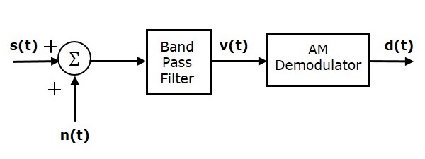
We know that the Amplitude Modulated (AM) wave is
$$s\left ( t \right )=A_c\left [ 1+k_am\left ( t \right ) \right ] \cos\left ( 2 \pi f_ct \right )$$
$$\Rightarrow s\left ( t \right )=A_c \cos \left ( 2 \pi f_ct \right )+A_ck_am\left ( t \right ) \cos\left ( 2 \pi f_ct \right )$$
Average power of AM wave is
$$P_s=\left ( \frac{A_c}{\sqrt{2}} \right )^2+\left ( \frac{A_ck_am\left ( t \right )}{\sqrt{2}} \right )^2=\frac{{A_{c}}^{2}}{2}+\frac{{A_{c}}^{2}{k_{a}}^{2}P}{2}$$
$$\Rightarrow P_s=\frac{{A_{c}}^{2}\left ( 1+{k_{a}}^{2}P \right )}{2}$$
Average power of noise in the message bandwidth is
$$P_{nc}=WN_0$$
Substitute, these values in channel SNR formula
$$\left ( SNR \right )_{C,AM}=\frac{Average \:\: Power \:\: of \:\: AM \:\: Wave}{Average \:\: Power \:\: of \:\: noise \:\: in \:\: message \:\: bandwidth}$$
$$\Rightarrow \left ( SNR \right )_{C,AM}=\frac{{A_{c}}^{2}\left ( 1+ {k_{a}}^{2}\right )P}{2WN_0}$$
Where,
P is the power of the message signal=$\frac{{A_{m}}^{2}}{2}$
W is the message bandwidth
Assume the band pass noise is mixed with AM wave in the channel as shown in the above figure. This combination is applied at the input of AM demodulator. Hence, the input of AM demodulator is.
$$v\left ( t \right )=s\left ( t \right )+n\left ( t \right )$$
$\Rightarrow v\left ( t \right )=A_c\left [ 1+k_am\left ( t \right ) \right ] \cos\left ( 2 \pi f_ct \right )+$
$\left [ n_1\left ( t \right ) \cos\left ( 2 \pi f_ct \right ) - n_Q\left ( t \right ) \sin \left ( 2 \pi f_ct \right )\right ]$
$\Rightarrow v\left ( t \right )=\left [ A_c+A_ck_am\left ( t \right )+n_1\left ( t \right ) \right ] \cos\left ( 2 \pi f_ct \right )-n_Q\left ( t \right ) \sin\left ( 2 \pi f_ct \right )$
Where $n_I \left ( t \right )$ and $n_Q \left ( t \right )$ are in phase and quadrature phase components of noise.
The output of AM demodulator is nothing but the envelope of the above signal.
$$d\left ( t \right )=\sqrt{\left [ A_c+A_cK_am\left ( t \right )+n_I\left ( t \right ) \right ]^2+\left ( n_Q\left ( t \right ) \right )^2}$$
$$\Rightarrow d\left ( t \right )\approx A_c+A_ck_am\left ( t \right )+n_1\left ( t \right )$$
Average power of the demodulated signal is
$$P_m=\left ( \frac{A_ck_am\left ( t \right )}{\sqrt{2}} \right )^2=\frac{{A_{c}}^{2}{k_{a}}^{2}P}{2}$$
Average power of noise at the output is
$$P_no=WN_0$$
Substitute, these values in output SNR formula.
$$\left ( SNR \right )_{O,AM}= \frac {Average \:\: Power \:\: of \:\: demodulated \:\: signal }{Average \:\: Power \:\: of \:\: noise \:\: at \:\: Output}$$
$$\Rightarrow \left ( SNR \right )_{O,AM}=\frac{{A_{c}}^{2}{k_{a}}^{2}P}{2WN_0}$$
Substitute, the values in Figure of merit of AM receiver formula.
$$F=\frac{\left ( SNR \right )_{O,AM}}{\left ( SNR \right )_{C,AM}}$$
$$\Rightarrow F=\left ( \frac{{A_{c}^{2}}{k_{a}^{2}}P}{2WN_0} \right )/\left ( \frac{{A_{c}}^{2}\left ( 1+ {k_{a}}^{2}\right )P}{2WN_0} \right )$$
$$\Rightarrow F=\frac{{K_{a}}^{2}P}{1+{K_{a}}^{2}P}$$
Therefore, the Figure of merit of AM receiver is less than one.
SNR Calculations in DSBSC System
Consider the following receiver model of DSBSC system to analyze noise.
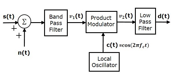
We know that the DSBSC modulated wave is
$$s\left ( t \right )=A_cm\left ( t \right ) \cos\left ( 2 \pi f_ct \right )$$
Average power of DSBSC modulated wave is
$$P_s=\left ( \frac{A_cm\left ( t \right )}{\sqrt{2}} \right )^2=\frac{{A_{c}}^{2}P}{2}$$
Average power of noise in the message bandwidth is
$$P_{nc}=WN_0$$
Substitute, these values in channel SNR formula.
$$\left ( SNR \right )_{C,DSBSC}=\frac{Average \:\: Power \:\: of \:\: DSBSC \:\: modulated \:\: wave}{Average \:\: Power \:\: of \:\: noise \:\: in \:\: message \:\: bandwidth}$$
$$\Rightarrow \left ( SNR \right )_{C,DSBSC}=\frac{{A_{c}}^{2}P}{2WN_0}$$
Assume the band pass noise is mixed with DSBSC modulated wave in the channel as shown in the above figure. This combination is applied as one of the input to the product modulator. Hence, the input of this product modulator is
$$v_1\left ( t \right )=s\left ( t \right )+n\left ( t \right )$$
$$\Rightarrow v_1\left ( t \right )=A_cm\left ( t \right ) \cos \left ( 2 \pi f_ct \right )+\left [ n_I\left ( t \right ) \cos\left ( 2 \pi f_ct \right ) - n_Q\left ( t \right ) \sin \left ( 2 \pi f_ct \right )\right ]$$
$$\Rightarrow v_1\left ( t \right )=\left [ A_cm \left ( t \right ) +n_I\left ( t \right ) \right ] \cos\left ( 2 \pi f_ct \right )-n_Q\left ( t \right ) \sin\left ( 2 \pi f_ct \right )$$
Local oscillator generates the carrier signal $c\left ( t \right )= \cos\left ( 2 \pi f_ct \right )$. This signal is applied as another input to the product modulator. Therefore, the product modulator produces an output, which is the product of $v_1\left ( t \right )$ and $c\left ( t \right )$.
$$v_2\left ( t \right )= v_1\left ( t \right )c\left ( t \right )$$
Substitute, $v_1\left ( t \right )$ and $c\left ( t \right )$ values in the above equation.
$$\Rightarrow v_2\left ( t \right )=\left ( \left [ A_cm\left ( t \right ) + n_I\left ( t \right )\right ] \cos\left ( 2 \pi f_ct \right )- n_Q\left ( t \right ) \sin\left ( 2 \pi f_ct \right ) \right ) \cos\left ( 2 \pi f_ct \right )$$
$$\Rightarrow v_2\left ( t \right )=\left [ A_c m\left ( t \right )+n_I\left ( t \right ) \right ] \cos^2\left ( 2 \pi f_ct \right )-n_Q\left ( t \right ) \sin\left ( 2 \pi f_ct \right ) \cos\left ( 2 \pi f_ct \right )$$
$$\Rightarrow v_2\left ( t \right )=\left [ A_c m\left ( t \right )+n_I\left ( t \right ) \right ] \left ( \frac{1+ \cos\left ( 4 \pi f_ct \right )}{2} \right ) -n_Q\left ( t \right )\frac{ \sin\left ( 4 \pi f_ct \right )}{2}$$
When the above signal is applied as an input to low pass filter, we will get the output of low pass filter as
$$d\left ( t \right )=\frac{\left [ A_c m\left ( t \right )+n_I\left ( t \right ) \right ]}{2}$$
Average power of the demodulated signal is
$$P_m=\left ( \frac{A_cm\left ( t \right )}{2\sqrt{2}} \right )^2=\frac{{A_{c}}^{2}P}{8}$$
Average power of noise at the output is
$$P_{no}=\frac{WN_0}{4}$$
Substitute, these values in output SNR formula.
$$\left ( SNR \right )_{O,DSBSC}= \frac {Average \:\: Power \:\: of \:\: demodulated \:\: signal }{Average \:\: Power \:\: of \:\: noise \:\: at \:\: Output}$$
$$\Rightarrow \left ( SNR \right )_{O,DSBSC}=\left ( \frac{{A_{c}}^{2}P}{8} \right )/ \left ( \frac{WN_0}{4} \right )=\frac{{A_{c}}^{2}P}{2WN_0}$$
Substitute, the values in Figure of merit of DSBSC receiver formula.
$$F=\frac{\left ( SNR \right )_{O,DSBSC}}{\left ( SNR \right )_{C,DSBSC}}$$
$$\Rightarrow F= \left ( \frac{{A_{c}}^{2}P}{2WN_0} \right )/ \left ( \frac{{A_{c}}^{2}P}{2WN_0} \right )$$
$$\Rightarrow F= 1$$
Therefore, the Figure of merit of DSBSC receiver is 1.
SNR Calculations in SSBSC System
Consider the following receiver model of SSBSC system to analyze noise.

We know that the SSBSC modulated wave having lower sideband is
$$s\left ( t \right )=\frac{A_mA_c}{2} \cos \left [ 2 \pi\left ( f_c-f_m \right )t \right ]$$
Average power of SSBSC modulated wave is
$$P_s=\left ( \frac{A_mA_c}{2\sqrt{2}} \right )^2=\frac{{A_{m}}^{2}{A_{c}}^{2}}{8}$$
Average power of noise in the message bandwidth is
$$P_{nc}=WN_0$$
Substitute, these values in channel SNR formula.
$$\left ( SNR \right )_{C,SSBSC}= \frac {Average \:\: Power \:\: of \:\: SSBSC \:\: modulated \:\: wave}{Average \:\: Power \:\: of \:\: noise \:\: in\:\: message \:\: bandwidth}$$
$$\Rightarrow \left ( SNR \right )_{C,SSBSC}=\frac{{A_{m}}^{2}{A_{c}}^{2}}{8WN_0}$$
Assume the band pass noise is mixed with SSBSC modulated wave in the channel as shown in the above figure. This combination is applied as one of the input to the product modulator. Hence, the input of this product modulator is
$$v_1\left ( t \right )=s\left ( t \right )+n\left ( t \right )$$
$$v_1\left ( t \right )=\frac{A_mA_c}{2} \cos\left [ 2 \pi \left ( f_c-f_m \right )t \right ] + n_I\left ( t \right ) \cos\left ( 2 \pi f_ct \right )-n_Q\left ( t \right ) \sin \left ( 2 \pi f_ct \right )$$
The local oscillator generates the carrier signal $c\left ( t \right )= \cos \left ( 2 \pi f_ct \right ) $. This signal is applied as another input to the product modulator. Therefore, the product modulator produces an output, which is the product of $v_1\left ( t \right )$ and $c\left ( t \right )$.
$$v_2\left ( t \right )=v_1\left ( t \right )c \left ( t \right )$$
Substitute, $v_1\left ( t \right )$ and $ c\left ( t \right )$ values in the above equation.
$\Rightarrow v_2(t)= (\frac{A_mA_c}{2} \cos[ 2 \pi ( f_c-f_m )t ] + n_I ( t ) \cos ( 2 \pi f_ct )-$
$n_Q( t ) \sin ( 2 \pi f_ct ) )\cos ( 2 \pi f_ct )$
$\Rightarrow v_2\left ( t \right )=\frac{A_mA_c}{2} \cos\left [ 2 \pi \left ( f_c-f_m \right )t \right ] \cos\left ( 2 \pi f_ct \right )+$
$n_I\left ( t \right ) \cos^2\left ( 2 \pi f_ct \right )-n_Q\left ( t \right ) \sin\left ( 2 \pi f_ct \right ) \cos\left ( 2 \pi f_ct \right )$
$\Rightarrow v_2\left ( t \right )=\frac{A_mA_c}{4} \left \{ \cos\left [ 2 \pi\left ( 2f_c-f_m \right )t \right ] + \cos \left ( 2 \pi f_mt \right )\right \}+$
$n_I\left ( t \right )\left ( \frac{1+ \cos\left ( 4 \pi f_ct \right )}{2} \right )- n_Q\left ( t \right )\frac{\sin \left ( 4 \pi f_ct \right )}{2}$
When the above signal is applied as an input to low pass filter, we will get the output of low pass filter as
$$d\left ( t \right )=\frac{A_mA_c}{2} \cos\left ( 2 \pi f_mt \right )+\frac{n_I\left ( t \right )}{2}$$
Average power of the demodulated signal is
$$P_m=\left ( \frac{A_mA_c}{4\sqrt{2}} \right )^2=\frac{{A_{m}}^{2}{A_{c}}^{2}}{32}$$
Average power of noise at the output is
$$P_{no}=\frac{WN_0}{4}$$
Substitute, these values in output SNR formula
$$\left ( SNR \right )_{O,SSBSC}= \frac {Average \:\: Power \:\: of \:\: demodulated \:\: signal}{Average \:\: Power \:\: of \:\: noise \:\: at \:\: output}$$
$$\Rightarrow \left ( SNR \right )_{O,SSBSC}= \left ( \frac{{A_{m}}^{2}{A_{c}}^{2}}{32} \right )/\left ( \frac{WN_0}{4} \right )=\frac{{A_{m}}^{2}{A_{c}}^{2}}{8WN_0}$$
Substitute, the values in Figure of merit of SSBSC receiver formula
$$F=\frac{\left ( SNR \right )_{O,SSBSC}}{\left ( SNR \right )_{C,SSBSC}}$$
$$F=\left ( \frac{{A_{m}}^{2}{A_{c}}^{2}}{8WN_0} \right )/\left ( \frac{{A_{m}}^{2}{A_{c}}^{2}}{8WN_0} \right )$$
$$F=1$$
Therefore, the Figure of merit of SSBSC receiver is 1.
Analog Communication - Transmitters
The antenna present at the end of transmitter section, transmits the modulated wave. In this chapter, let us discuss about AM and FM transmitters.
AM Transmitter
AM transmitter takes the audio signal as an input and delivers amplitude modulated wave to the antenna as an output to be transmitted. The block diagram of AM transmitter is shown in the following figure.
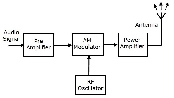
The working of AM transmitter can be explained as follows.
The audio signal from the output of the microphone is sent to the pre-amplifier, which boosts the level of the modulating signal.
The RF oscillator generates the carrier signal.
Both the modulating and the carrier signal is sent to AM modulator.
Power amplifier is used to increase the power levels of AM wave. This wave is finally passed to the antenna to be transmitted.
FM Transmitter
FM transmitter is the whole unit, which takes the audio signal as an input and delivers FM wave to the antenna as an output to be transmitted. The block diagram of FM transmitter is shown in the following figure.
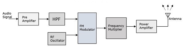
The working of FM transmitter can be explained as follows.
The audio signal from the output of the microphone is sent to the pre-amplifier, which boosts the level of the modulating signal.
This signal is then passed to high pass filter, which acts as a pre-emphasis network to filter out the noise and improve the signal to noise ratio.
This signal is further passed to the FM modulator circuit.
The oscillator circuit generates a high frequency carrier, which is sent to the modulator along with the modulating signal.
Several stages of frequency multiplier are used to increase the operating frequency. Even then, the power of the signal is not enough to transmit. Hence, a RF power amplifier is used at the end to increase the power of the modulated signal. This FM modulated output is finally passed to the antenna to be transmitted.
Analog Communication - Receivers
The antenna present at the beginning of the receiver section, receives the modulated wave. First let us discuss the requirements of a receiver.
Requirements of a Receiver
AM receiver receives AM wave and demodulates it by using the envelope detector. Similarly, FM receiver receives FM wave and demodulates it by using the Frequency Discrimination method. Following are the requirements of both AM and FM receiver.
It should be cost-effective.
It should receive the corresponding modulated waves.
The receiver should be able to tune and amplify the desired station.
It should have an ability to reject the unwanted stations.
Demodulation has to be done to all the station signals, irrespective of the carrier signal frequency.
For these requirements to be fulfilled, the tuner circuit and the mixer circuit should be very effective. The procedure of RF mixing is an interesting phenomenon.
RF Mixing
The RF mixing unit develops an Intermediate Frequency (IF) to which any received signal is converted, so as to process the signal effectively.
RF Mixer is an important stage in the receiver. Two signals of different frequencies are taken where one signal level affects the level of the other signal, to produce the resultant mixed output. The input signals and the resultant mixer output is illustrated in the following figures.
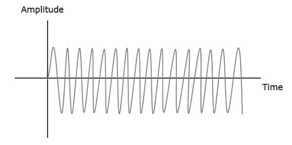
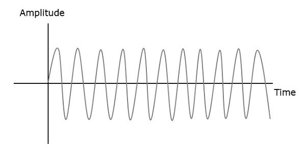
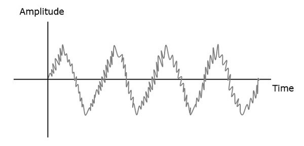
Let the first and second signal frequencies be $f_1$ and $f_2$. If these two signals are applied as inputs of RF mixer, then it produces an output signal, having frequencies of $f_1+f_2$ and $f_1-f_2$.
If this is observed in the frequency domain, the pattern looks like the following figure.
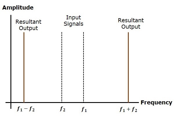
In this case, $f_1$ is greater than $f_2$. So, the resultant output has frequencies $f_1+f_2$ and $f_1-f_2$. Similarly, if $f_2$ is greater than $f_1$, then the resultant output will have the frequencies $f_1+f_2$ and $f_1-f_2$.
AM Receiver
The AM super heterodyne receiver takes the amplitude modulated wave as an input and produces the original audio signal as an output. Selectivity is the ability of selecting a particular signal, while rejecting the others. Sensitivity is the capacity of detecting RF signal and demodulating it, while at the lowest power level.
Radio amateurs are the initial radio receivers. However, they have drawbacks such as poor sensitivity and selectivity. To overcome these drawbacks, super heterodyne receiver was invented. The block diagram of AM receiver is shown in the following figure.
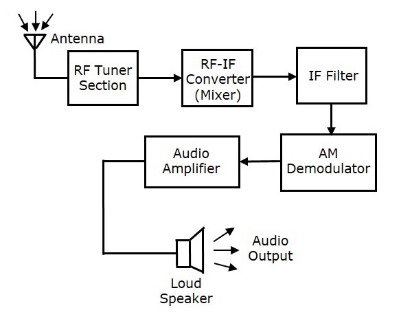
RF Tuner Section
The amplitude modulated wave received by the antenna is first passed to the tuner circuit through a transformer. The tuner circuit is nothing but a LC circuit, which is also called as resonant or tank circuit. It selects the frequency, desired by the AM receiver. It also tunes the local oscillator and the RF filter at the same time.
RF Mixer
The signal from the tuner output is sent to the RF-IF converter, which acts as a mixer. It has a local oscillator, which produces a constant frequency. The mixing process is done here, having the received signal as one input and the local oscillator frequency as the other input. The resultant output is a mixture of two frequencies $\left [ \left ( f_1+f_2 \right ) , \left ( f_1-f_2 \right )\right ]$ produced by the mixer, which is called as the Intermediate Frequency (IF).
The production of IF helps in the demodulation of any station signal having any carrier frequency. Hence, all signals are translated to a fixed carrier frequency for adequate selectivity.
IF Filter
Intermediate frequency filter is a band pass filter, which passes the desired frequency. It eliminates all other unwanted frequency components present in it. This is the advantage of IF filter, which allows only IF frequency.
AM Demodulator
The received AM wave is now demodulated using AM demodulator. This demodulator uses the envelope detection process to receive the modulating signal.
Audio Amplifier
This is the power amplifier stage, which is used to amplify the detected audio signal. The processed signal is strengthened to be effective. This signal is passed on to the loudspeaker to get the original sound signal.
FM Receiver
The block diagram of FM receiver is shown in the following figure.
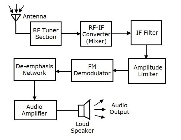
This block diagram of FM receiver is similar to the block diagram of AM receiver. The two blocks Amplitude limiter and De-emphasis network are included before and after FM demodulator. The operation of the remaining blocks is the same as that of AM receiver.
We know that in FM modulation, the amplitude of FM wave remains constant. However, if some noise is added with FM wave in the channel, due to that the amplitude of FM wave may vary. Thus, with the help of amplitude limiter we can maintain the amplitude of FM wave as constant by removing the unwanted peaks of the noise signal.
In FM transmitter, we have seen the pre-emphasis network (High pass filter), which is present before FM modulator. This is used to improve the SNR of high frequency audio signal. The reverse process of pre-emphasis is known as de-emphasis. Thus, in this FM receiver, the de-emphasis network (Low pass filter) is included after FM demodulator. This signal is passed to the audio amplifier to increase the power level. Finally, we get the original sound signal from the loudspeaker.
Analog Communication - Sampling
So far, we have discussed about continuous-wave modulation. We will discuss about pulse modulation in the next chapter. These pulse modulation techniques deal with discrete signals. So, now let us see how to convert a continuous time signal into a discrete one.
The process of converting continuous time signals into equivalent discrete time signals, can be termed as Sampling. A certain instant of data is continually sampled in the sampling process.
The following figure shows a continuous-time signal x(t) and the corresponding sampled signal xs(t). When x(t) is multiplied by a periodic impulse train, the sampled signal xs(t) is obtained.
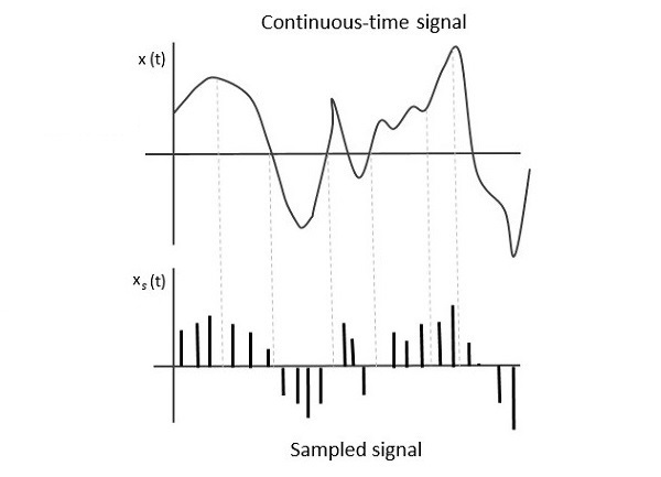
A sampling signal is a periodic train of pulses, having unit amplitude, sampled at equal intervals of time $T_s$, which is called as sampling time. This data is transmitted at the time instants $T_s$ and the carrier signal is transmitted at the remaining time.
Sampling Rate
To discretize the signals, the gap between the samples should be fixed. That gap can be termed as the sampling period $T_s$. Reciprocal of the sampling period is known as sampling frequency or sampling rate $f_s$.
Mathematically, we can write it as
$$f_s= \frac{1}{T_s}$$
Where,
$f_s$ is the sampling frequency or the sampling rate
$T_s$ is the sampling period
Sampling Theorem
The sampling rate should be such that the data in the message signal should neither be lost nor it should get over-lapped. The sampling theorem states that, a signal can be exactly reproduced if it is sampled at the rate $f_s$, which is greater than or equal to twice the maximum frequency of the given signal W.
Mathematically, we can write it as
$$f_s\geq 2W$$
Where,
$f_s$ is the sampling rate
$W$ is the highest frequency of the given signal
If the sampling rate is equal to twice the maximum frequency of the given signal W, then it is called as Nyquist rate.
The sampling theorem, which is also called as Nyquist theorem, delivers the theory of sufficient sample rate in terms of bandwidth for the class of functions that are bandlimited.
For continuous-time signal x(t), which is band-limited in the frequency domain is represented as shown in the following figure.
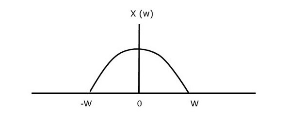
If the signal is sampled above Nyquist rate, then the original signal can be recovered. The following figure explains a signal, if sampled at a higher rate than 2w in the frequency domain.
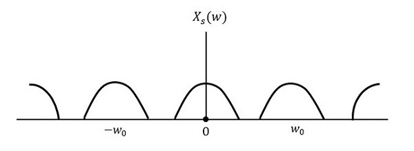
If the same signal is sampled at a rate less than 2w, then the sampled signal would look like the following figure.
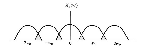
We can observe from the above pattern that there is over-lapping of information, which leads to mixing up and loss of information. This unwanted phenomenon of over-lapping is called as Aliasing.
Aliasing can be referred to as the phenomenon of a high-frequency component in the spectrum of a signal, taking on the identity of a low-frequency component in the spectrum of its sampled version.
Hence, the sampling rate of the signal is chosen to be as Nyquist rate. If the sampling rate is equal to twice the highest frequency of the given signal W, then the sampled signal would look like the following figure.
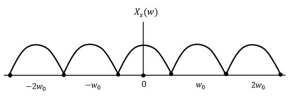
In this case, the signal can be recovered without any loss. Hence, this is a good sampling rate.
Analog Communication - Pulse Modulation
After continuous wave modulation, the next division is Pulse modulation. In this chapter, let us discuss the following analog pulse modulation techniques.
- Pulse Amplitude Modulation
- Pulse Width Modulation
- Pulse Position Modulation
Pulse Amplitude Modulation
In Pulse Amplitude Modulation (PAM) technique, the amplitude of the pulse carrier varies, which is proportional to the instantaneous amplitude of the message signal.
The pulse amplitude modulated signal will follow the amplitude of the original signal, as the signal traces out the path of the whole wave. In natural PAM, a signal sampled at Nyquist rate can be reconstructed, by passing it through an efficient Low Pass Filter (LPF) with exact cutoff frequency.
The following figures explain the Pulse Amplitude Modulation.
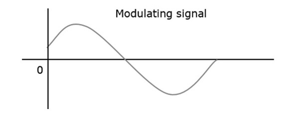
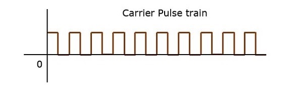
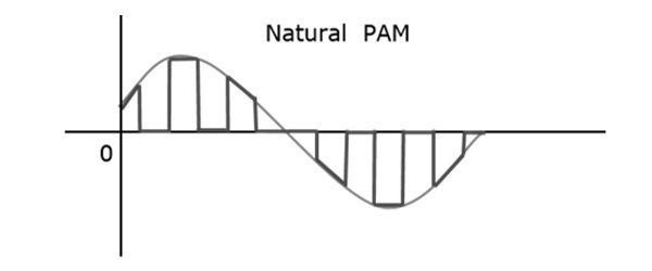
Though the PAM signal is passed through a LPF, it cannot recover the signal without distortion. Hence, to avoid this noise, use flat-top sampling. The flat-top PAM signal is shown in the following figure.
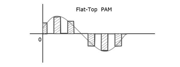
Flat-top sampling is the process in which, the sampled signal can be represented in pulses for which the amplitude of the signal cannot be changed with respect to the analog signal, to be sampled. The tops of amplitude remain flat. This process simplifies the circuit design.
Pulse Width Modulation
In Pulse Width Modulation (PWM) or Pulse Duration Modulation (PDM) or Pulse Time Modulation (PTM) technique, the width or the duration or the time of the pulse carrier varies, which is proportional to the instantaneous amplitude of the message signal.
The width of the pulse varies in this method, but the amplitude of the signal remains constant. Amplitude limiters are used to make the amplitude of the signal constant. These circuits clip off the amplitude to a desired level, and hence the noise is limited.
The following figure explains the types of Pulse Width Modulations.
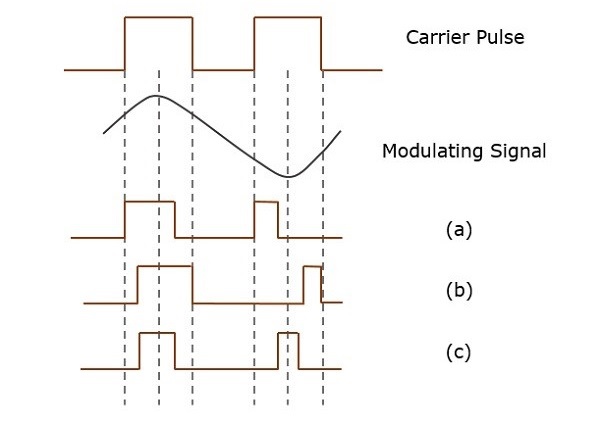
There are three types of PWM.
The leading edge of the pulse being constant, the trailing edge varies according to the message signal. The waveform for this type of PWM is denoted as (a) in the above figure.
The trailing edge of the pulse being constant, the leading edge varies according to the message signal. The waveform for this type of PWM is denoted as (b) in the above figure.
The center of the pulse being constant, the leading edge and the trailing edge varies according to the message signal. The waveform for this type of PWM is denoted as (c) shown in the above figure.
Pulse Position Modulation
Pulse Position Modulation (PPM) is an analog modulation scheme in which, the amplitude and the width of the pulses are kept constant, while the position of each pulse, with reference to the position of a reference pulse varies according to the instantaneous sampled value of the message signal.
The transmitter has to send synchronizing pulses (or simply sync pulses) to keep the transmitter and the receiver in sync. These sync pulses help to maintain the position of the pulses. The following figures explain the Pulse Position Modulation.
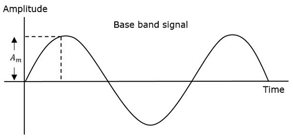
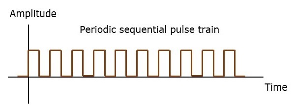
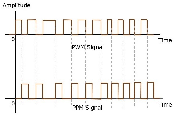
Pulse position modulation is done in accordance with the pulse width modulated signal. Each trailing edge of the pulse width modulated signal becomes the starting point for pulses in PPM signal. Hence, the position of these pulses is proportional to the width of the PWM pulses.
Advantage
As the amplitude and the width are constant, the power handled is also constant.
Disadvantage
The synchronization between the transmitter and the receiver is a must.
Comparison between PAM, PWM, and PPM
The following table presents the comparison between three modulation techniques.
| PAM | PWM | PPM |
|---|---|---|
| Amplitude is varied | Width is varied | Position is varied |
| Bandwidth depends on the width of the pulse | Bandwidth depends on the rise time of the pulse | Bandwidth depends on the rise time of the pulse |
| Instantaneous transmitter power varies with the amplitude of the pulses | Instantaneous transmitter power varies with the amplitude and the width of the pulses | Instantaneous transmitter power remains constant with the width of the pulses |
| System complexity is high | System complexity is low | System complexity is low |
| Noise interference is high | Noise interference is low | Noise interference is low |
| It is similar to amplitude modulation | It is similar to frequency modulation | It is similar to phase modulation |
Analog Communication - Transducers
Transducer is a device, which converts energy from one form to other. In this chapter, let us discuss about the transducers used in communication systems.
Why do We Need Transducers?
In the real world, communication between any two nearby persons takes place with the help of sound waves. But, if the persons are far away, then it is difficult to convey the information without any loss by using sound waves in its physical form.
To overcome this difficulty, we can use modulators in the transmitter section and demodulators in the receiver section. These modulators and demodulators operate with electrical signals. Thats why we require a device, which has to convert the sound waves into electrical signals or vice versa. That device is known as a transducer.
Following is a simple block diagram of a transducer.
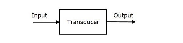
This transducer has a single input and a single output. It converts the energy present at the input into its equivalent output having another energy. Basically, a transducer converts the non-electrical form of energy into an electrical form or vice versa.
Types of Transducers
We can classify the transducers into following two types based on the placement (position) of the transducer in communication systems.
- Input Transducer
- Output Transducer
Input Transducers
The transducer present at the input of the communication system is known as an input transducer. Following is the block diagram of an input transducer.
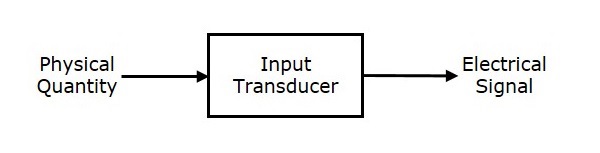
This input transducer converts the non-electrical physical quantity into an electrical signal. The physical quantities such as sound or light can be converted into electrical quantities such as voltage or current by using this transducer. Example: Microphone.
Microphone is used as the input transducer, which is placed between the information source and the transmitter section. The information source produces the information in the form of sound waves. The microphone converts these sound waves into electrical signals with the help of a diaphragm. These electrical signals can be used for further processing.
Output Transducers
The transducer present at the output of communication system is known as output transducer. Following is the block diagram of an output transducer.
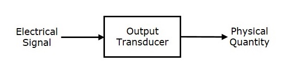
This output transducer converts the electrical signal into non-electrical physical quantity. The electrical quantities such as voltage or current can be converted into physical quantities such as sound or light by using this transducer. Example: Loudspeaker.
The loud speaker is used as the output transducer, which is placed between the receiver section and the destination. The demodulator present in the receiver section produces the demodulated output. So, the loud speaker converts the electrical signals (demodulated output) into sound waves. Therefore, the functionality of the loud speaker is just opposite to the functionality of the microphone.
In addition to the above transducers, there is one more transducer which is used in communication systems. This transducer can be placed either at the end of the transmitter section or at the starting of the receiver section. Example: Antenna.
An Antenna is a transducer, which converts electrical signals into electromagnetic waves and vice versa. An Antenna can be used either as a transmitting antenna or as a receiving antenna.
A transmitting antenna converts electrical signals into electromagnetic waves and radiates them. While, a receiving antenna converts electromagnetic waves from the received beam into electrical signals.
In this two-way communication, the same antenna can be used for both transmission and reception.
