- Analog Communication - Home
- Introduction
- Modulation
- Amplitude Modulation
- Numerical Problems 1
- AM Modulators
- AM Demodulators
- DSBSC Modulation
- DSBSC Modulators
- DSBSC Demodulators
- SSBSC Modulation
- SSBSC Modulators
- SSBSC Demodulator
- VSBSC Modulation
- Angle Modulation
- Numerical Problems 2
- FM Modulators
- FM Demodulators
- Multiplexing
- Noise
- SNR Calculations
- Transmitters
- Receivers
- Sampling
- Pulse Modulation
- Transducers
Analog Communication - DSBSC Modulators
In this chapter, let us discuss about the modulators, which generate DSBSC wave. The following two modulators generate DSBSC wave.
- Balanced modulator
- Ring modulator
Balanced Modulator
Following is the block diagram of the Balanced modulator.
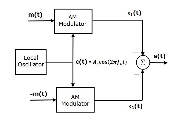
Balanced modulator consists of two identical AM modulators. These two modulators are arranged in a balanced configuration in order to suppress the carrier signal. Hence, it is called as Balanced modulator.
The same carrier signal $c\left ( t \right )= A_c \cos \left ( 2 \pi f_ct \right )$ is applied as one of the inputs to these two AM modulators. The modulating signal $m\left ( t \right )$ is applied as another input to the upper AM modulator. Whereas, the modulating signal $m\left ( t \right )$ with opposite polarity, i.e., $-m\left ( t \right )$ is applied as another input to the lower AM modulator.
Output of the upper AM modulator is
$$s_1\left ( t \right )=A_c\left [1+k_am\left ( t \right ) \right ] \cos\left ( 2 \pi f_ct \right )$$
Output of the lower AM modulator is
$$s_2\left ( t \right )=A_c\left [1-k_am\left ( t \right ) \right ] \cos\left ( 2 \pi f_ct \right )$$
We get the DSBSC wave $s\left ( t \right )$ by subtracting $s_2\left ( t \right )$ from $s_1\left ( t \right )$. The summer block is used to perform this operation. $s_1\left ( t \right )$ with positive sign and $s_2\left ( t \right )$ with negative sign are applied as inputs to summer block. Thus, the summer block produces an output $s\left ( t \right )$ which is the difference of $s_1\left ( t \right )$ and $s_2\left ( t \right )$.
$$\Rightarrow s\left ( t \right )=A_c\left [ 1+k_am\left ( t \right ) \right ] \cos\left ( 2 \pi f_ct \right )-A_c\left [ 1-k_am\left ( t \right ) \right ] \cos\left ( 2 \pi f_ct \right )$$
$$\Rightarrow s\left ( t \right )=A_c \cos\left ( 2 \pi f_ct \right )+A_ck_am\left ( t \right ) \cos\left ( 2 \pi f_ct \right )- A_c \cos\left ( 2 \pi f_ct \right )+$$
$A_ck_am\left ( t \right ) \cos\left ( 2 \pi f_ct \right )$
$\Rightarrow s\left ( t \right )=2A_ck_am\left ( t \right ) \cos\left ( 2 \pi f_ct \right )$
We know the standard equation of DSBSC wave is
$$s\left ( t \right )=A_cm \left ( t \right ) \cos\left ( 2 \pi f_ct \right )$$
By comparing the output of summer block with the standard equation of DSBSC wave, we will get the scaling factor as $2k_a$
Ring Modulator
Following is the block diagram of the Ring modulator.
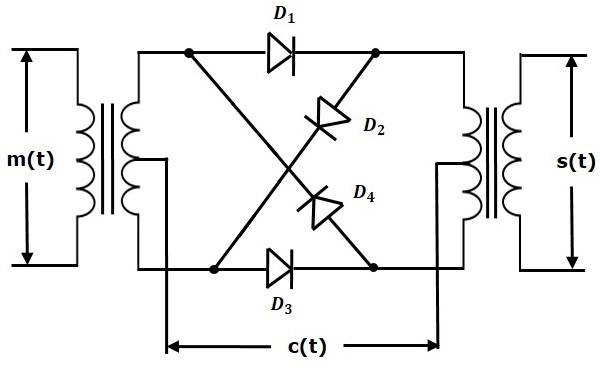
In this diagram, the four diodes $D_1$,$D_2$,$D_3$ and $D_4$ are connected in the ring structure. Hence, this modulator is called as the ring modulator. Two center tapped transformers are used in this diagram. The message signal $m\left ( t \right )$ is applied to the input transformer. Whereas, the carrier signals $c\left ( t \right )$ is applied between the two center tapped transformers.
For positive half cycle of the carrier signal, the diodes $D_1$ and $D_3$ are switched ON and the other two diodes $D_2$ and $D_4$ are switched OFF. In this case, the message signal is multiplied by +1.
For negative half cycle of the carrier signal, the diodes $D_2$ and $D_4$ are switched ON and the other two diodes $D_1$ and $D_3$ are switched OFF. In this case, the message signal is multiplied by -1. This results in $180^0$ phase shift in the resulting DSBSC wave.
From the above analysis, we can say that the four diodes $D_1$, $D_2$, $D_3$ and $D_4$ are controlled by the carrier signal. If the carrier is a square wave, then the Fourier series representation of $c\left ( t \right )$ is represented as
$$c\left ( t \right )=\frac{4}{\pi}\sum_{n=1}^{\infty }\frac{\left ( -1 \right )^{n-1}}{2n-1} \cos\left [2 \pi f_ct\left ( 2n-1 \right ) \right ]$$
We will get DSBSC wave $s\left ( t \right )$, which is just the product of the carrier signal $c\left ( t \right )$ and the message signal $m\left ( t \right )$ i.e.,
$$s\left ( t \right )=\frac{4}{\pi}\sum_{n=1}^{\infty }\frac{\left ( -1 \right )^{n-1}}{2n-1} \cos\left [2 \pi f_ct\left ( 2n-1 \right ) \right ]m\left ( t \right )$$
The above equation represents DSBSC wave, which is obtained at the output transformer of the ring modulator.
DSBSC modulators are also called as product modulators as they produce the output, which is the product of two input signals.
