- Transistors - Overview
- Transistor Configurations
- Transistor Regions of Operation
- Transistor Load Line Analysis
- Operating Point
- Transistor as an Amplifier
- Transistor Biasing
- Methods of Transistor Biasing
- Bias Compensation
- Amplifiers
- Basic Amplifier
- Classification of Amplifiers
- Based on Configurations
- Multi-Stage Transistor Amplifier
- RC Coupling Amplifier
- Transformer Coupled Amplifier
- Direct Coupled Amplifier
- Power Amplifiers
- Classification of Power Amplifiers
- Class A Power Amplifiers
- Transformer Coupled Class A Power Amplifier
- Push-Pull Class A Power Amplifier
- Class B Power Amplifier
- Class AB and C Power Amplifiers
- Tuned Amplifiers
- Types of Tuned Amplifiers
- Feedback Amplifiers
- Negative Feedback Amplifiers
- Emitter Follower & Darlington Amplifier
- Noise in Amplifiers
- Amplifiers Useful Resources
- Amplifiers - Quick Guide
- Amplifiers - Useful Resources
- Amplifiers - Discussion
Transistor Load Line Analysis
Till now we have discussed different regions of operation for a transistor. But among all these regions, we have found that the transistor operates well in active region and hence it is also called as linear region. The outputs of the transistor are the collector current and collector voltages.
Output Characteristics
When the output characteristics of a transistor are considered, the curve looks as below for different input values.
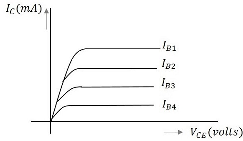
In the above figure, the output characteristics are drawn between collector current IC and collector voltage VCE for different values of base current IB. These are considered here for different input values to obtain different output curves.
Load Line
When a value for the maximum possible collector current is considered, that point will be present on the Y-axis, which is nothing but the Saturation point. As well, when a value for the maximum possible collector emitter voltage is considered, that point will be present on the X-axis, which is the Cutoff point.
When a line is drawn joining these two points, such a line can be called as Load line. This is called so as it symbolizes the output at the load. This line, when drawn over the output characteristic curve, makes contact at a point called as Operating point or quiescent point or simply Q-point.
The concept of load line can be understood from the following graph.
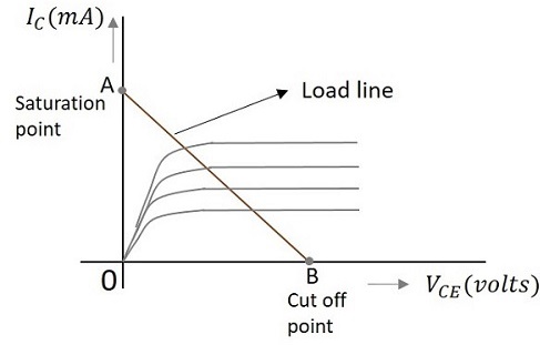
The load line is drawn by joining the saturation and cut off points. The region that lies between these two is the linear region. A transistor acts as a good amplifier in this linear region.
If this load line is drawn only when DC biasing is given to the transistor, but no input signal is applied, then such a load line is called as DC load line. Whereas the load line drawn under the conditions when an input signal along with the DC voltages are applied, such a line is called as an AC load line.
DC Load Line
When the transistor is given the bias and no signal is applied at its input, the load line drawn under such conditions, can be understood as DC condition. Here there will be no amplification as the signal is absent. The circuit will be as shown below.
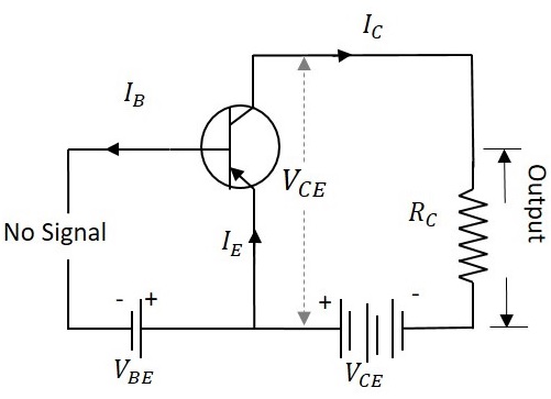
The value of collector emitter voltage at any given time will be
$$V_{CE} = V_{CC} - I_C R_C$$
As VCC and RC are fixed values, the above one is a first degree equation and hence will be a straight line on the output characteristics. This line is called as D.C. Load line. The figure below shows the DC load line.
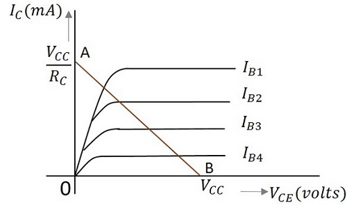
To obtain the load line, the two end points of the straight line are to be determined. Let those two points be A and B.
To obtain A
When collector emitter voltage VCE = 0, the collector current is maximum and is equal to VCC/RC. This gives the maximum value of VCE. This is shown as
$$V_{CE} = V_{CC} - I_C R_C$$
$$0 = V_{CC} - I_C R_C$$
$$I_C = V_{CC}/R_C$$
This gives the point A (OA = VCC/RC) on collector current axis, shown in the above figure.
To obtain B
When the collector current IC = 0, then collector emitter voltage is maximum and will be equal to the VCC. This gives the maximum value of IC. This is shown as
$$V_{CE} = V_{CC} - I_C R_C$$
$$= V_{CC}$$
(AS IC = 0)
This gives the point B, which means (OB = VCC) on the collector emitter voltage axis shown in the above figure.
Hence we got both the saturation and cutoff point determined and learnt that the load line is a straight line. So, a DC load line can be drawn.
AC Load Line
The DC load line discussed previously, analyzes the variation of collector currents and voltages, when no AC voltage is applied. Whereas the AC load line gives the peak-to-peak voltage, or the maximum possible output swing for a given amplifier.
We shall consider an AC equivalent circuit of a CE amplifier for our understanding.
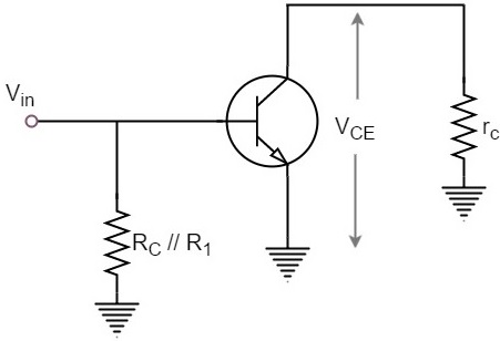
From the above figure,
$$V_{CE} = (R_C // R_1) \times I_C$$
$$r_C = R_C // R_1$$
For a transistor to operate as an amplifier, it should stay in active region. The quiescent point is so chosen in such a way that the maximum input signal excursion is symmetrical on both negative and positive half cycles.
Hence,
$V_{max} = V_{CEQ}$ and $V_{min} = -V_{CEQ}$
Where VCEQ is the emitter-collector voltage at quiescent point
The following graph represents the AC load line which is drawn between saturation and cut off points.
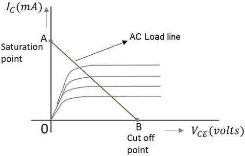
From the graph above, the current IC at the saturation point is
$$I_{C(sat)} = I_{CQ} + (V_{CEQ}/r_C)$$
The voltage VCE at the cutoff point is
$$V_{CE(off)} = V_{CEQ} + I_{CQ}r_C$$
Hence the maximum current for that corresponding VCEQ = VCEQ / (RC // R1) is
$$I_{CQ} = I_{CQ} * (R_C // R_1)$$
Hence by adding quiescent currents the end points of AC load line are
$$I_{C(sat)} = I_{CQ} + V_{CEQ}/ (R_C // R_1)$$
$$V_{CE(off)} = V_{CEQ} + I_{CQ} * (R_C // R_1)$$
AC and DC Load Line
When AC and DC Load lines are represented in a graph, it can be understood that they are not identical. Both of these lines intersect at the Q-point or quiescent point. The endpoints of AC load line are saturation and cut off points. This is understood from the figure below.
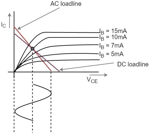
From the above figure, it is understood that the quiescent point (the dark dot) is obtained when the value of base current IB is 10mA. This is the point where both the AC and DC load lines intersect.
In the next chapter, we will discuss the concept of quiescent point or the operating point in detail.
