- Transistors - Overview
- Transistor Configurations
- Transistor Regions of Operation
- Transistor Load Line Analysis
- Operating Point
- Transistor as an Amplifier
- Transistor Biasing
- Methods of Transistor Biasing
- Bias Compensation
- Amplifiers
- Basic Amplifier
- Classification of Amplifiers
- Based on Configurations
- Multi-Stage Transistor Amplifier
- RC Coupling Amplifier
- Transformer Coupled Amplifier
- Direct Coupled Amplifier
- Power Amplifiers
- Classification of Power Amplifiers
- Class A Power Amplifiers
- Transformer Coupled Class A Power Amplifier
- Push-Pull Class A Power Amplifier
- Class B Power Amplifier
- Class AB and C Power Amplifiers
- Tuned Amplifiers
- Types of Tuned Amplifiers
- Feedback Amplifiers
- Negative Feedback Amplifiers
- Emitter Follower & Darlington Amplifier
- Noise in Amplifiers
- Amplifiers Useful Resources
- Amplifiers - Quick Guide
- Amplifiers - Useful Resources
- Amplifiers - Discussion
Transistor Configurations
Any transistor has three terminals, the emitter, the base, and the collector. Using these 3 terminals the transistor can be connected in a circuit with one terminal common to both input and output in three different possible configurations.
The three types of configurations are Common Base, Common Emitter and Common Collector configurations. In every configuration, the emitter junction is forward biased and the collector junction is reverse biased.
Common Base (CB) Configuration
The name itself implies that the Base terminal is taken as common terminal for both input and output of the transistor. The common base connection for both NPN and PNP transistors is as shown in the following figure.
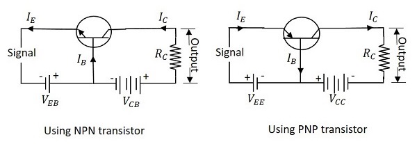
For the sake of understanding, let us consider NPN transistor in CB configuration. When the emitter voltage is applied, as it is forward biased, the electrons from the negative terminal repel the emitter electrons and current flows through the emitter and base to the collector to contribute collector current. The collector voltage VCB is kept constant throughout this.
In the CB configuration, the input current is the emitter current IE and the output current is the collector current IC.
Current Amplification Factor (α)
The ratio of change in collector current (ΔIC) to the change in emitter current (ΔIE) when collector voltage VCB is kept constant, is called as Current amplification factor. It is denoted by α.
$\alpha = \frac{\Delta I_C}{\Delta I_E}$ at constant VCB
Expression for Collector current
With the above idea, let us try to draw some expression for collector current.
Along with the emitter current flowing, there is some amount of base current IB which flows through the base terminal due to electron hole recombination. As collector-base junction is reverse biased, there is another current which is flown due to minority charge carriers. This is the leakage current which can be understood as Ileakage. This is due to minority charge carriers and hence very small.
The emitter current that reaches the collector terminal is
$$\alpha I_E$$
Total collector current
$$I_C = \alpha I_E + I_{leakage}$$
If the emitter-base voltage VEB = 0, even then, there flows a small leakage current, which can be termed as ICBO (collector-base current with output open).
The collector current therefore can be expressed as
$$I_C = \alpha I_E + I_{CBO}$$
$$I_E = I_C + I_B$$
$$I_C = \alpha (I_C + I_B) + I_{CBO}$$
$$I_C (1 - \alpha) = \alpha I_B + I_{CBO}$$
$$I_C = \frac{\alpha}{1 - \alpha}I_B + \frac{I_{CBO}}{1 - \alpha}$$
$$I_C = \left ( \frac{\alpha}{1 - \alpha} \right )I_B + \left ( \frac{1}{1 - \alpha} \right )I_{CBO}$$
Hence the above derived is the expression for collector current. The value of collector current depends on base current and leakage current along with the current amplification factor of that transistor in use.
Characteristics of CB configuration
This configuration provides voltage gain but no current gain.
Being VCB constant, with a small increase in the Emitter-base voltage VEB, Emitter current IE gets increased.
Emitter Current IE is independent of Collector voltage VCB.
Collector Voltage VCB can affect the collector current IC only at low voltages, when VEB is kept constant.
The input resistance Ri is the ratio of change in emitter-base voltage (ΔVEB) to the change in emitter current (ΔIE) at constant collector base voltage VCB.
$R_i = \frac{\Delta V_{EB}}{\Delta I_E}$ at constant VCB
As the input resistance is of very low value, a small value of VEB is enough to produce a large current flow of emitter current IE.
The output resistance Ro is the ratio of change in the collector base voltage (ΔVCB) to the change in collector current (ΔIC) at constant emitter current IE.
$R_o = \frac{\Delta V_{CB}}{\Delta I_C}$ at constant IE
As the output resistance is of very high value, a large change in VCB produces a very little change in collector current IC.
This Configuration provides good stability against increase in temperature.
The CB configuration is used for high frequency applications.
Common Emitter (CE) Configuration
The name itself implies that the Emitter terminal is taken as common terminal for both input and output of the transistor. The common emitter connection for both NPN and PNP transistors is as shown in the following figure.
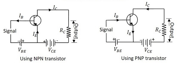
Just as in CB configuration, the emitter junction is forward biased and the collector junction is reverse biased. The flow of electrons is controlled in the same manner. The input current is the base current IB and the output current is the collector current IC here.
Base Current Amplification factor (β)
The ratio of change in collector current (ΔIC) to the change in base current (ΔIB) is known as Base Current Amplification Factor. It is denoted by β.
$$\beta = \frac{\Delta I_C}{\Delta I_B}$$
Relation between β and α
Let us try to derive the relation between base current amplification factor and emitter current amplification factor.
$$\beta = \frac{\Delta I_C}{\Delta I_B}$$
$$\alpha = \frac{\Delta I_C}{\Delta I_E}$$
$$I_E = I_B + I_C$$
$$\Delta I_E = \Delta I_B + \Delta I_C$$
$$\Delta I_B = \Delta I_E - \Delta I_C$$
We can write
$$\beta = \frac{\Delta I_C}{\Delta I_E - \Delta I_C}$$
Dividing by ΔIE
$$\beta = \frac{\Delta I_C/\Delta I_E}{\frac{\Delta I_E}{\Delta I_E} - \frac{\Delta I_C}{\Delta I_E}}$$
We have
$$\alpha = \Delta I_C / \Delta I_E$$
Therefore,
$$\beta = \frac{\alpha}{1 - \alpha}$$
From the above equation, it is evident that, as α approaches 1, β reaches infinity.
Hence, the current gain in Common Emitter connection is very high. This is the reason this circuit connection is mostly used in all transistor applications.
Expression for Collector Current
In the Common Emitter configuration, IB is the input current and IC is the output current.
We know
$$I_E = I_B + I_C$$
And
$$I_C = \alpha I_E + I_{CBO}$$
$$= \alpha(I_B + I_C) + I_{CBO}$$
$$I_C(1 - \alpha) = \alpha I_B + I_{CBO}$$
$$I_C = \frac{\alpha}{1 - \alpha}I_B + \frac{1}{1 - \alpha}I_{CBO}$$
If base circuit is open, i.e. if IB = 0,
The collector emitter current with base open is ICEO
$$I_{CEO} = \frac{1}{1 - \alpha}I_{CBO}$$
Substituting the value of this in the previous equation, we get
$$I_C = \frac{\alpha}{1 - \alpha}I_B + I_{CEO}$$
$$I_C = \beta I_B + I_{CEO}$$
Hence the equation for collector current is obtained.
Knee Voltage
In CE configuration, by keeping the base current IB constant, if VCE is varied, IC increases nearly to 1v of VCE and stays constant thereafter. This value of VCE up to which collector current IC changes with VCE is called the Knee Voltage. The transistors while operating in CE configuration, they are operated above this knee voltage.
Characteristics of CE Configuration
This configuration provides good current gain and voltage gain.
Keeping VCE constant, with a small increase in VBE the base current IB increases rapidly than in CB configurations.
For any value of VCE above knee voltage, IC is approximately equal to βIB.
The input resistance Ri is the ratio of change in base emitter voltage (ΔVBE) to the change in base current (ΔIB) at constant collector emitter voltage VCE.
$R_i = \frac{\Delta V_{BE}}{\Delta I_B}$ at constant VCE
As the input resistance is of very low value, a small value of VBE is enough to produce a large current flow of base current IB.
The output resistance Ro is the ratio of change in collector emitter voltage (ΔVCE) to the change in collector current (ΔIC) at constant IB.
$R_o = \frac{\Delta V_{CE}}{\Delta I_C}$ at constant IB
As the output resistance of CE circuit is less than that of CB circuit.
This configuration is usually used for bias stabilization methods and audio frequency applications.
Common Collector (CC) Configuration
The name itself implies that the Collector terminal is taken as common terminal for both input and output of the transistor. The common collector connection for both NPN and PNP transistors is as shown in the following figure.
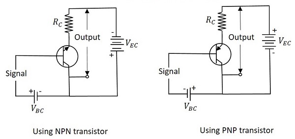
Just as in CB and CE configurations, the emitter junction is forward biased and the collector junction is reverse biased. The flow of electrons is controlled in the same manner. The input current is the base current IB and the output current is the emitter current IE here.
Current Amplification Factor (γ)
The ratio of change in emitter current (ΔIE) to the change in base current (ΔIB) is known as Current Amplification factor in common collector (CC) configuration. It is denoted by γ.
$$\gamma = \frac{\Delta I_E}{\Delta I_B}$$
- The current gain in CC configuration is same as in CE configuration.
- The voltage gain in CC configuration is always less than 1.
Relation between γ and α
Let us try to draw some relation between γ and α
$$\gamma = \frac{\Delta I_E}{\Delta I_B}$$
$$\alpha = \frac{\Delta I_C}{\Delta I_E}$$
$$I_E = I_B + I_C$$
$$\Delta I_E = \Delta I_B + \Delta I_C$$
$$\Delta I_B = \Delta I_E - \Delta I_C$$
Substituting the value of IB, we get
$$\gamma = \frac{\Delta I_E}{\Delta I_E - \Delta I_C}$$
Dividing by ΔIE
$$\gamma = \frac{\Delta I_E / \Delta I_E}{\frac{\Delta I_E}{\Delta I_E} - \frac{\Delta I_C}{\Delta I_E}}$$
$$= \frac{1}{1 - \alpha}$$
$$\gamma = \frac{1}{1 - \alpha}$$
Expression for collector current
We know
$$I_C = \alpha I_E + I_{CBO}$$
$$I_E = I_B + I_C = I_B + (\alpha I_E + I_{CBO})$$
$$I_E(1 - \alpha) = I_B + I_{CBO}$$
$$I_E = \frac{I_B}{1 - \alpha} + \frac{I_{CBO}}{1 - \alpha}$$
$$I_C \cong I_E = (\beta + 1)I_B + (\beta + 1)I_{CBO}$$
The above is the expression for collector current.
Characteristics of CC Configuration
This configuration provides current gain but no voltage gain.
In CC configuration, the input resistance is high and the output resistance is low.
The voltage gain provided by this circuit is less than 1.
The sum of collector current and base current equals emitter current.
The input and output signals are in phase.
This configuration works as non-inverting amplifier output.
This circuit is mostly used for impedance matching. That means, to drive a low impedance load from a high impedance source.
