- Transistors - Overview
- Transistor Configurations
- Transistor Regions of Operation
- Transistor Load Line Analysis
- Operating Point
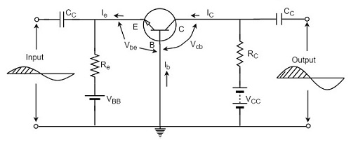
- Transistor as an Amplifier
- Transistor Biasing
- Methods of Transistor Biasing
- Bias Compensation
- Amplifiers
- Basic Amplifier
- Classification of Amplifiers
- Based on Configurations
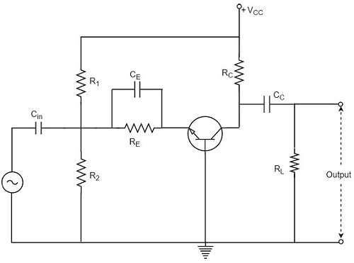
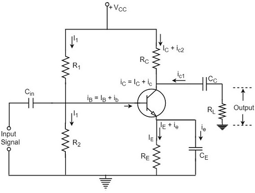
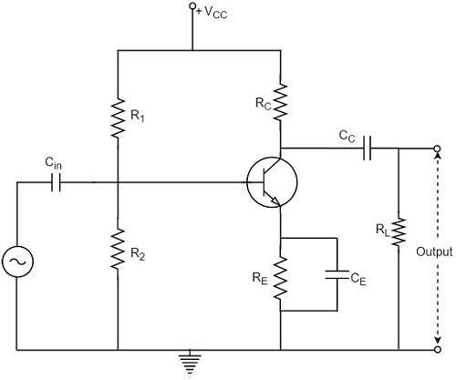
- Multi-Stage Transistor Amplifier
- RC Coupling Amplifier
- Transformer Coupled Amplifier
- Direct Coupled Amplifier
- Power Amplifiers
- Classification of Power Amplifiers
- Class A Power Amplifiers
- Transformer Coupled Class A Power Amplifier
- Push-Pull Class A Power Amplifier
- Class B Power Amplifier
- Class AB and C Power Amplifiers
- Tuned Amplifiers
- Types of Tuned Amplifiers
- Feedback Amplifiers
- Negative Feedback Amplifiers
- Emitter Follower & Darlington Amplifier
- Noise in Amplifiers
- Amplifiers Useful Resources
- Amplifiers - Quick Guide
- Amplifiers - Useful Resources
- Amplifiers - Discussion
Based on Configurations
Any transistor amplifier, uses a transistor to amplify the signals which is connected in one of the three configurations. For an amplifier it is a better state to have a high input impedance, in order to avoid loading effect in Multi-stage circuits and lower output impedance, in order to deliver maximum output to the load. The voltage gain and power gain should also be high to produce a better output.
Let us now study different configurations to understand which configuration suits better for a transistor to work as an amplifier.
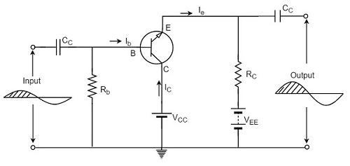
CB Amplifier
The amplifier circuit that is formed using a CB configured transistor combination is called as CB amplifier.
Construction
The common base amplifier circuit using NPN transistor is as shown below, the input signal being applied at emitter base junction and the output signal being taken from collector base junction.
The emitter base junction is forward biased by VEE and collector base junction is reverse biased by VCC. The operating point is adjusted with the help of resistors Re and Rc. Thus the values of Ic, Ib and Icb are decided by VCC, VEE, Re and Rc.
Operation
When no input is applied, the quiescent conditions are formed and no output is present. As Vbe is at negative with respect to ground, the forward bias is decreased, for the positive half of the input signal. As a result of this, the base current IB also gets decreased.
The below figure shows the CB amplifier with self-bias circuit.
As we know that,
$$I_C \cong I_E \cong \beta I_B$$
Both the collector current and emitter current get decreased.
The voltage drop across RC is
$$V_C = I_C R_C$$
This VC also gets decreased.
As ICRC decreases, VCB increases. It is because,
$$V_{CB} = V_{CC} - I_C R_C$$
Thus, a positive half cycle output is produced.
In CB configuration, a positive input produces a positive output and hence input and output are in phase. So, there is no phase reversal between input and output in a CB amplifier.
If CB configuration is considered for amplification, it has low input impedance and high output impedance. The voltage gain is also low compared to CE configuration. Hence CB configured amplifiers are used at high frequency applications.
CE Amplifier
The amplifier circuit that is formed using a CE configured transistor combination is called as CE amplifier.
Construction
The common emitter amplifier circuit using NPN transistor is as shown below, the input signal being applied at emitter base junction and the output signal being taken from collector base junction.
The emitter base junction is forward biased by VEE and collector base junction is reverse biased by VCC. The operating point is adjusted with the help of resistors Re and Rc. Thus the values of Ic, Ib and Icb are decided by VCC, VEE, Re and Rc.
Operation
When no input is applied, the quiescent conditions are formed and no output is present. When positive half of the signal is being applied, the voltage between base and emitter Vbe is increased because it is already positive with respect to ground.
As forward bias increases, the base current too increases accordingly. Since IC = βIB, the collector current increases as well.
The following circuit diagram shows a CE amplifier with self-bias circuit.
The collector current when flows through RC, the voltage drop increases.
$$V_C = I_C R_C$$
As a consequence of this, the voltage between collector and emitter decreases. Because,
$$V_{CB} = V_{CC} - I_C R_C$$
Thus, the amplified voltage appears across RC.
Therefore, in a CE amplifier, as the positive going signal appears as a negative going signal, it is understood that there is a phase shift of 180o between input and output.
CE amplifier has a high input impedance and lower output impedance than CB amplifier. The voltage gain and power gain are also high in CE amplifier and hence this is mostly used in Audio amplifiers.
CC Amplifier
The amplifier circuit that is formed using a CC configured transistor combination is called as CC amplifier.
Construction
The common collector amplifier circuit using NPN transistor is as shown below, the input signal being applied at base collector junction and the output signal being taken from emitter collector junction.
The emitter base junction is forward biased by VEE and collector base junction is reverse biased by VCC. The Q-values of Ib and Ie are adjusted by Rb and Re.
Operation
When no input is applied, the quiescent conditions are formed and no output is present. When positive half of the signal is being applied, the forward bias is increased because Vbe is positive with respect to collector or ground. With this, the base current IB and the collector current IC are increased.
The following circuit diagram shows a CC amplifier with self-bias circuit.
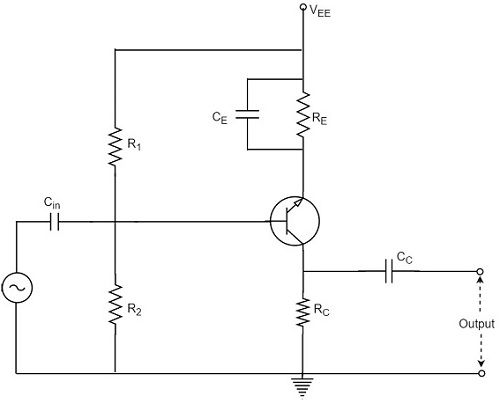
Consequently, the voltage drop across Re i.e. the output voltage is increased. As a result, positive half cycle is obtained. As the input and output are in phase, there is no phase reversal.
If CC configuration is considered for amplification, though CC amplifier has better input impedance and lower output impedance than CE amplifier, the voltage gain of CC is very less which limits its applications to impedance matching only.
Comparison between CB CE CC Amplifiers
Let us compare the characteristic details of CB, CE, and CC amplifiers.
| Characteristic | CE | CB | CC |
|---|---|---|---|
| Input resistance | Low (1K to 2K) | Very low (30-150 Ω) | High (20-500 KΩ) |
| Output resistance | Large (≈ 50 K) | High (≈ 500 K) | Low (50-1000 KΩ) |
| Current gain | B high | α < 1 | High (1 + β) |
| Voltage gain | High (≈ 1500) | High (≈ 1500) | Less than one |
| Power gain | High (≈ 10,000) | High (≈ 7500) | Low (250-500) |
| Phase between input and output | reversed | same | same |
Due to the compatibility and characteristic features, the common-emitter configuration is mostly used in amplifier circuits.
