- Transistors - Overview
- Transistor Configurations
- Transistor Regions of Operation
- Transistor Load Line Analysis
- Operating Point
- Transistor as an Amplifier
- Transistor Biasing
- Methods of Transistor Biasing
- Bias Compensation
- Amplifiers
- Basic Amplifier
- Classification of Amplifiers
- Based on Configurations
- Multi-Stage Transistor Amplifier
- RC Coupling Amplifier
- Transformer Coupled Amplifier
- Direct Coupled Amplifier
- Power Amplifiers
- Classification of Power Amplifiers
- Class A Power Amplifiers
- Transformer Coupled Class A Power Amplifier
- Push-Pull Class A Power Amplifier
- Class B Power Amplifier
- Class AB and C Power Amplifiers
- Tuned Amplifiers
- Types of Tuned Amplifiers
- Feedback Amplifiers
- Negative Feedback Amplifiers
- Emitter Follower & Darlington Amplifier
- Noise in Amplifiers
- Amplifiers Useful Resources
- Amplifiers - Quick Guide
- Amplifiers - Useful Resources
- Amplifiers - Discussion
Materials - Introduction
Every material in nature has certain properties. These properties define the behavior of the materials. Material Science is a branch of electronics that deals with the study of flow of electrons in various materials or spaces, when they are subjected to various conditions.
Due to the intermixing of atoms in solids, instead of single energy levels, there will be bands of energy levels formed. These set of energy levels, which are closely packed are called as Energy bands.
Types of Materials
The energy band in which valence electrons are present is called Valence band, while the band in which conduction electrons are present is called Conduction band. The energy gap between these two bands is called as Forbidden energy gap.
Electronically, the materials are broadly classified as Insulators, Semiconductors, and Conductors.
Insulators − Insulators are such materials in which the conduction cannot take place, due to the large forbidden gap. Examples: Wood, Rubber.
Semiconductors − Semiconductors are such materials in which the forbidden energy gap is small and the conduction takes place if some external energy is applied. Examples: Silicon, Germanium.
Conductors − Conductors are such materials in which the forbidden energy gap disappears as the valence band and conduction band become very close that they overlap. Examples: Copper, Aluminum.
Of all the three, insulators are used where resistivity to electricity is desired and conductors are used where the conduction has to be high. The semiconductors are the ones which give rise to a specific interest of how they are used.
Semiconductors
A Semiconductor is a substance whose resistivity lies between the conductors and insulators. The property of resistivity is not the only one that decides a material as a semiconductor, but it has few properties as follows.
Semiconductors have the resistivity which is less than insulators and more than conductors.
Semiconductors have negative temperature co-efficient. The resistance in semiconductors, increases with the decrease in temperature and vice versa.
The Conducting properties of a Semi-conductor changes, when a suitable metallic impurity is added to it, which is a very important property.
The Semiconductor devices are extensively used in the field of electronics. The transistor has replaced the bulky vacuum tubes, from which the size and cost of the devices got decreased and this revolution has kept on increasing its pace leading to the new inventions like integrated electronics. Semiconductors can be classified as shown below.
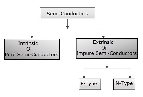
A semiconductor in its extremely pure form is said to be an intrinsic semiconductor. But the conduction capability of this pure form is too low. In order to increase the conduction capability of intrinsic semiconductor, it is better to add some impurities. This process of adding impurities is called as Doping. Now, this doped intrinsic semiconductor is called as an Extrinsic Semiconductor.
The impurities added, are generally pentavalent and trivalent impurities. Depending upon these types of impurities, another classification is done. When a pentavalent impurity is added to a pure semiconductor, it is called as N-type extrinsic Semiconductor. As well, when a trivalent impurity is added to a pure semiconductor, it is called as P-type extrinsic Semiconductor.
P-N Junction
When an electron moves from its place, a hole is said to be formed there. So, a hole is the absence of an electron. If an electron is said to be moved from negative to positive terminal, it means that a hole is being moved from positive to negative terminal.
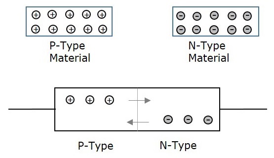
The materials mentioned above are the basics of semiconductor technology. The N-type material formed by adding pentavalent impurities has electrons as its majority carriers and holes as minority carriers. While, the P-type material formed by adding trivalent impurities has holes as its majority carriers and electrons as minority carriers.
Let us try to understand what happens when the P and N materials are joined together.
If a P-type and an N-type material are brought close to each other, both of them join to form a junction, as shown in the figure below.
A P-type material has holes as the majority carriers and an N-type material has electrons as the majority carriers. As opposite charges attract, few holes in P-type tend to go to n-side, whereas few electrons in N-type tend to go to P-side.
As both of them travel towards the junction, holes and electrons recombine with each other to neutralize and forms ions. Now, in this junction, there exists a region where the positive and negative ions are formed, called as PN junction or junction barrier as shown in the figure.
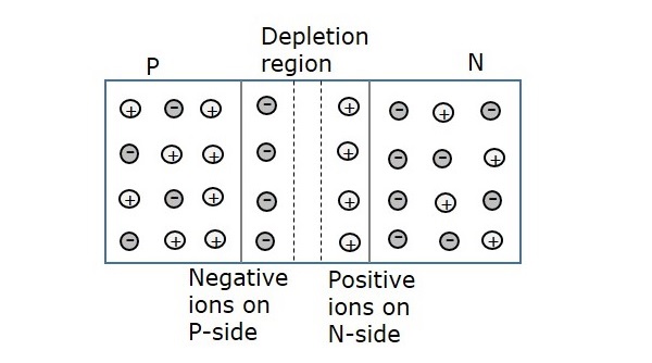
The formation of negative ions on P-side and positive ions on N-side results in the formation of a narrow charged region on either side of the PN junction. This region is now free from movable charge carriers. The ions present here have been stationary and maintain a region of space between them without any charge carriers.
As this region acts as a barrier between P and N type materials, this is also called as Barrier junction. This has another name called as Depletion region meaning it depletes both the regions. There occurs a potential difference VD due to the formation of ions, across the junction called as Potential Barrier as it prevents further movement of holes and electrons through the junction. This formation is called as a Diode.
Biasing of a Diode
When a diode or any two terminal components are connected in a circuit, it has two biased conditions with the given supply. They are Forward biased condition and Reverse biased condition.
Forward Biased Condition
When a diode is connected in a circuit, with its anode to the positive terminal and cathode to the negative terminal of the supply, then such a connection is said to be forward biased condition.
This kind of connection makes the circuit more and more forward biased and helps in more conduction. A diode conducts well in forward biased condition.
Reverse Biased Condition
When a diode is connected in a circuit, with its anode to the negative terminal and cathode to the positive terminal of the supply, then such a connection is said to be Reverse biased condition.
This kind of connection makes the circuit more and more reverse biased and helps in minimizing and preventing the conduction. A diode cannot conduct in reverse biased condition.
With the above information, we now have a good idea of what a PN junction is. With this knowledge, let us move on and learn about transistors in the next chapter.
