- Transistors - Overview
- Transistor Configurations
- Transistor Regions of Operation
- Transistor Load Line Analysis
- Operating Point
- Transistor as an Amplifier
- Transistor Biasing
- Methods of Transistor Biasing
- Bias Compensation
- Amplifiers
- Basic Amplifier
- Classification of Amplifiers
- Based on Configurations
- Multi-Stage Transistor Amplifier
- RC Coupling Amplifier
- Transformer Coupled Amplifier
- Direct Coupled Amplifier
- Power Amplifiers
- Classification of Power Amplifiers
- Class A Power Amplifiers
- Transformer Coupled Class A Power Amplifier
- Push-Pull Class A Power Amplifier
- Class B Power Amplifier
- Class AB and C Power Amplifiers
- Tuned Amplifiers
- Types of Tuned Amplifiers
- Feedback Amplifiers
- Negative Feedback Amplifiers
- Emitter Follower & Darlington Amplifier
- Noise in Amplifiers
- Amplifiers Useful Resources
- Amplifiers - Quick Guide
- Amplifiers - Useful Resources
- Amplifiers - Discussion
Class A Power Amplifiers
We have already come across the details of transistor biasing, which is very important for the operation of a transistor as an amplifier. Hence to achieve faithful amplification, the biasing of the transistor has to be done such that the amplifier operates over the linear region.
A Class A power amplifier is one in which the output current flows for the entire cycle of the AC input supply. Hence the complete signal present at the input is amplified at the output. The following figure shows the circuit diagram for Class A Power amplifier.
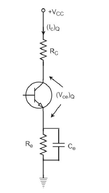
From the above figure, it can be observed that the transformer is present at the collector as a load. The use of transformer permits the impedance matching, resulting in the transference of maximum power to the load e.g. loud speaker.
The operating point of this amplifier is present in the linear region. It is so selected that the current flows for the entire ac input cycle. The below figure explains the selection of operating point.
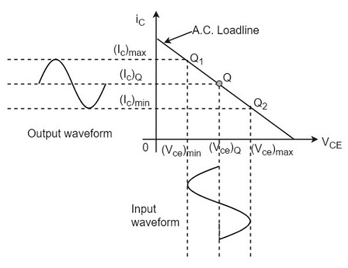
The output characteristics with operating point Q is shown in the figure above. Here (Ic)Q and (Vce)Q represent no signal collector current and voltage between collector and emitter respectively. When signal is applied, the Q-point shifts to Q1 and Q2. The output current increases to (Ic)max and decreases to (Ic)min. Similarly, the collector-emitter voltage increases to (Vce)max and decreases to (Vce)min.
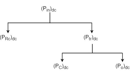
D.C. Power drawn from collector battery Vcc is given by
$$P_{in} = voltage \times current = V_{CC}(I_C)_Q$$
This power is used in the following two parts −
- Power dissipated in the collector load as heat is given by
$$P_{RC} = (current)^2 \times resistance = (I_C)^2_Q R_C$$
- Power given to transistor is given by
$$P_{tr} = P_{in} - P_{RC} = V_{CC} - (I_C)^2_Q R_C$$
When signal is applied, the power given to transistor is used in the following two parts −
A.C. Power developed across load resistors RC which constitutes the a.c. power output.
$$(P_O)_{ac} = I^2 R_C = \frac{V^2}{R_C} = \left ( \frac{V_m}{\sqrt{2}}\right )^2 \frac{1}{R_C} = \frac{V_m^2}{2R_C}$$
Where I is the R.M.S. value of a.c. output current through load, V is the R.M.S. value of a.c. voltage, and Vm is the maximum value of V.
The D.C. power dissipated by the transistor (collector region) in the form of heat, i.e., (PC)dc
We have represented the whole power flow in the following diagram.
This class A power amplifier can amplify small signals with least distortion and the output will be an exact replica of the input with increased strength.
Let us now try to draw some expressions to represent efficiencies.
Overall Efficiency
The overall efficiency of the amplifier circuit is given by
$$(\eta)_{overall} = \frac{a.c \: power \:delivered\: to \: the\: load}{total \: power\: delivered \: by \: d.c\: supply}$$
$$= \frac{(P_O)_{ac}}{(P_{in})_{dc}}$$
Collector Efficiency
The collector efficiency of the transistor is defined as
$$(\eta)_{collector} = \frac{average\: a.c \: power \:output}{average \:d.c\: power\: input\: to\: transistor}$$
$$= \frac{(P_O)_{ac}}{(P_{tr})_{dc}}$$
Expression for overall efficiency
$$(P_O)_{ac} = V_{rms} \times I_{rms}$$
$$= \frac{1}{\sqrt{2}} \left [ \frac{(V_{ce})_{max} - (V_{ce})_{min}}{2} \right ] \times \frac{1}{\sqrt{2}} \left [ \frac{(I_C)_{max} - (I_C)_{min}}{2}\right ]$$
$$= \frac{[(V_{ce})_{max} - (V_{ce})_{min}] \times [(I_C)_{max} - (I_C)_{min}]}{8}$$
Therefore
$$(\eta)_{overall} = \frac{[(V_{ce})_{max} - (V_{ce})_{min}] \times [(I_C)_{max} - (I_C)_{min}]}{8 \times V_{CC} (I_C)_Q}$$
Advantages of Class A Amplifiers
The advantages of Class A power amplifier are as follows −
- The current flows for complete input cycle
- It can amplify small signals
- The output is same as input
- No distortion is present
Disadvantages of Class A Amplifiers
The advantages of Class A power amplifier are as follows −
- Low power output
- Low collector efficiency