- Pulse Circuits Time Base Generators
- Time Base Generators (Overview)
- Types of Time Base Generators
- Bootstrap Time Base Generator
- Miller Sweep Generator
- Pulse Circuits Sweep Circuits
- Unijunction Transistor
- UJT as Relaxation Oscillator
- Pulse Circuits - Synchronization
- Pulse Circuits - Blocking Oscillators
- Pulse Circuits Sampling Gates
- Pulse Circuits - Sampling Gates
- Unidirectional Sampling Gate
- Unidirectional with More Inputs
- Bidirectional Sampling Gates
- Pulse Circuits Useful Resources
- Pulse Circuits - Quick Guide
- Pulse Circuits - Useful Resources
- Pulse Circuits - Discussion
Pulse Circuits - Unijunction Transistor
Unijunction Transistor is such a transistor that has a single PN junction, but still not a diode. Unijunction Transistor, or simply UJT has an emitter and two bases, unlike a normal transistor. This component is especially famous for its negative resistance property and also for its application as a relaxation oscillator.
Construction of UJT
A bar of highly resistive n-type silicon, is considered to form the base structure. Two Ohmic contacts are drawn at both the ends being both the bases. An aluminum rod like structure is attached to it which becomes the emitter. This emitter lies near to the base 2 and a bit far to the base1. Both of these join to form a PN junction. As single PN junction is present, this component is called as a Unijunction transistor.
An internal resistance called as intrinsic resistance is present inside the bar whose resistance value depends upon the doping concentration of the bar. The construction and symbol of UJT are as shown below.
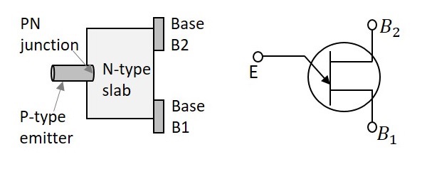
In the symbol, the emitter is indicated by an inclined arrow and the remaining two ends indicate the bases. As the UJT is understood as a combination of diode and some resistance, the internal structure of UJT can be indicated by an equivalent diagram to explain the working of UJT.
Working of UJT
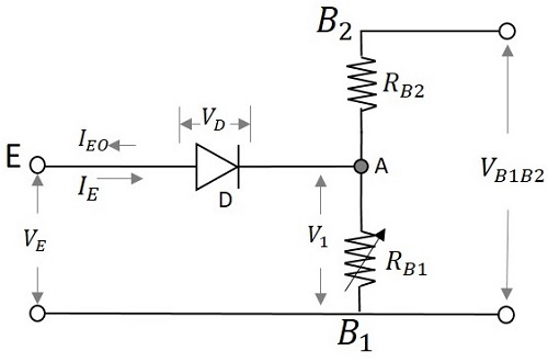
The working of UJT can be understood by its equivalent circuit. The voltage applied at the emitter is indicated as VE and the internal resistances are indicated as RB1 and RB2 at bases 1 and 2 respectively. Both resistances present internally are together called as intrinsic resistance, indicated as RBB. The voltage across RB1 can be denoted as V1. The dc voltage applied for the circuit to function is VBB.
The UJT equivalent circuit is as given below.
Initially when no voltage is applied,
$$V_E = 0$$
Then the voltage VBB is applied through RB2. The diode D will be in reverse bias. The voltage across the diode will be VB which is the barrier voltage of the emitter diode. Due to the application of VBB, some voltage appears at point A. So, the total voltage will be VA + VB.
Now if the emitter voltage VE is increased, the current IE flows through the diode D. This current makes the diode forward biased. The carriers get induced and the resistance RB1 goes on decreasing. Therefore, the potential across RB1 which means VB1 also decreases.
$$V_{B1} = \left( \frac{R_{B1}}{R_{B1} + R_{B2}} \right )V_{BB}$$
As VBB is constant and RB1 decreases to its minimum value due to the doping concentration of the channel, VB1 also decreases.
Actually, the resistances present internally are together called as intrinsic resistance, indicated as RBB. The resistance mentioned above can be indicated as
$$R_{BB} = R_{B1} + R_{B2}$$
$$\left( \frac{R_{B1}}{R_{BB}} \right ) = \eta$$
The symbol η is used to represent the total resistance applied.
Hence voltage across VB1 is represented as
$$V_{B1} = \eta V_{BB}$$
The emitter voltage is given as
$$V_E = V_D + V_{B1}$$
$$V_E = 0.7 + V_{B1}$$
Where VD is the voltage across the diode.
As the diode gets forward biased, the voltage across it will be 0.7v. So, this is constant and VB1 goes on decreasing. Hence VE goes on decreasing. It decreases to a least value which may be denoted VV called as Valley voltage. The voltage at which the UJT gets switched ON is the Peak Voltage denoted as VP.
V-I Characteristics of UJT
The concept discussed till now is clearly understood from the following graph shown below.
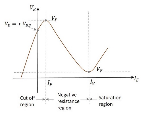
Initially when VE is zero, some reverse current IE flows until, the value of VE reaches a point at which
$$V_E = \eta V_{BB}$$
This is the point where the curve touches the Y-axis.
When VE reaches a voltage where
$$V_E = \eta V_{BB} + V_D$$
At this point, the diode gets forward biased.
The voltage at this point is called as VP (Peak Voltage) and the current at this point is called as IP (Peak Current). The portion in the graph till now, is termed as Cut off region as the UJT was in OFF state.
Now, when VE is further increased, the resistance RB1 and then the voltage V1 also decreases, but the current through it increases. This is the Negative resistance property and hence this region is called as Negative resistance region.
Now, the voltage VE reaches a certain point where further increase leads to the increase in voltage across RB1. The voltage at this point is called as VV (Valley Voltage) and the current at this point is called as IV (Valley Current). The region after this is termed as Saturation region.
Applications of UJT
UJTs are most prominently used as relaxation oscillators. They are also used in Phase Control Circuits. In addition, UJTs are widely used to provide clock for digital circuits, timing control for various devices, controlled firing in thyristors, and sync pulsed for horizontal deflection circuits in CRO.
