- Pulse Circuits Time Base Generators
- Time Base Generators (Overview)
- Types of Time Base Generators
- Bootstrap Time Base Generator
- Miller Sweep Generator
- Pulse Circuits Sweep Circuits
- Unijunction Transistor
- UJT as Relaxation Oscillator
- Pulse Circuits - Synchronization
- Pulse Circuits - Blocking Oscillators
- Pulse Circuits Sampling Gates
- Pulse Circuits - Sampling Gates
- Unidirectional Sampling Gate
- Unidirectional with More Inputs
- Bidirectional Sampling Gates
- Pulse Circuits Useful Resources
- Pulse Circuits - Quick Guide
- Pulse Circuits - Useful Resources
- Pulse Circuits - Discussion
Pulse Circuits - Transistor as a Switch
A transistor is used as an electronic switch by driving it either in saturation or in cut off. The region between these two is the linear region. A transistor works as a linear amplifier in this region. The Saturation and Cut off states are important consideration in this regard.
ON & OFF States of a Transistor
There are two main regions in the operation of a transistor which we can consider as ON and OFF states. They are saturation and cut off states. Let us have a look at the behavior of a transistor in those two states.
Operation in Cut-off condition
The following figure shows a transistor in cut-off region.
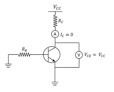
When the base of the transistor is given negative, the transistor goes to cut off state. There is no collector current. Hence IC = 0.
The voltage VCC applied at the collector, appears across the collector resistor RC. Therefore,
VCE = VCC
Operation in Saturation region
The following figure shows a transistor in saturation region.
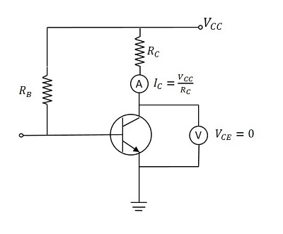
When the base voltage is positive and transistor goes into saturation, IC flows through RC.
Then VCC drops across RC. The output will be zero.
$$I_C = I_{C(sat)} \: = \: \frac{V_{CC}}{R_C} \: and \: V_{CE} = 0$$
Actually, this is the ideal condition. Practically, some leakage current flows. Hence we can understand that a transistor works as a switch when driven into saturation and cut off regions by applying positive and negative voltages to the base.
The following figure gives a better explanation.
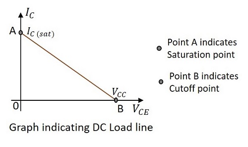
Observe the dc load line that connects the IC and VCC. If the transistor is driven into saturation, IC flows completely and VCE = 0 which is indicated by the point A.
If the transistor is driven into cut off, IC will be zero and VCE = VCC which is indicated by the point B. the line joining the saturation point A and cut off B is called as Load line. As the voltage applied here is dc, it is called as DC Load line.
Practical Considerations
Though the above-mentioned conditions are all convincing, there are a few practical limitations for such results to occur.
During the Cut off state
An ideal transistor has VCE = VCC and IC = 0.
But in practice, a smaller leakage current flows through the collector.
Hence IC will be a few μA.
This is called as Collector Leakage Current which is of course, negligible.
During the Saturation State
An ideal transistor has VCE = 0 and IC = IC(sat).
But in practice, VCE decreases to some value called knee voltage.
When VCE decreases more than knee voltage, β decreases sharply.
As IC = βIB this decreases the collector current.
Hence that maximum current IC which maintains VCE at knee voltage, is known as Saturation Collector Current.
Saturation Collector Current = $I_{C(sat)} \: = \: \frac{V_{CC} - V_{knee}}{R_C}$
A Transistor which is fabricated only to make it work for switching purposes is called as Switching Transistor. This works either in Saturation or in Cut off region. While in saturation state, the collector saturation current flows through the load and while in cut off state, the collector leakage current flows through the load.
Switching Action of a Transistor
A Transistor has three regions of operation. To understand the efficiency of operation, the practical losses are to be considered. So let us try to get an idea on how efficiently a transistor works as a switch.
During Cut off (OFF) state
The Base current IB = 0
The Collector current IC = ICEO (collector lekeage current)
Power Loss = Output Voltage × Output Current
$$= V_{CC} \times I_{CEO}$$
As ICEO is very small and VCC is also low, the loss will be of very low value. Hence, a transistor works as an efficient switch in OFF state.
During Saturation (ON) state
As discussed earlier,
$$I_{C(sat)} = \frac{V_{CC} - V_{knee}}{R_C}$$
The output voltage is Vknee.
Power loss = Output Voltage × Output Current
$$= \:V_{knee} \times I_{c(sat)}$$
As Vknee will be of small value, the loss is low. Hence, a transistor works as an efficient switch in ON state.
During Active region
The transistor lies between ON & OFF states. The transistor operates as a linear amplifier where small changes in input current cause large changes in the output current (ΔIC).
Switching Times
The Switching transistor has a pulse as an input and a pulse with few variations will be the output. There are a few terms that you should know regarding the timings of the switching output pulse. Let us go through them.
Let the input pulse duration = T
When the input pulse is applied the collector current takes some time to reach the steady state value, due to the stray capacitances. The following figure explains this concept.
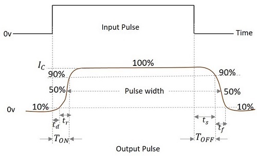
From the figure above,
Time delay(td) − The time taken by the collector current to reach from its initial value to 10% of its final value is called as the Time Delay.
Rise time(tr) − The time taken for the collector current to reach from 10% of its initial value to 90% of its final value is called as the Rise Time.
Turn-on time (TON) − The sum of time delay (td) and rise time (tr) is called as Turn-on time.
TON = td + tr
Storage time (ts) − The time interval between the trailing edge of the input pulse to the 90% of the maximum value of the output, is called as the Storage time.
Fall time (tf) − The time taken for the collector current to reach from 90% of its maximum value to 10% of its initial value is called as the Fall Time.
Turn-off time (TOFF) − The sum of storage time (ts) and fall time (tf) is defined as the Turn-off time.
TOFF = ts + tf
Pulse Width(W) − The time duration of the output pulse measured between two 50% levels of rising and falling waveform is defined as Pulse Width.
