- Pulse Circuits Time Base Generators
- Time Base Generators (Overview)
- Types of Time Base Generators
- Bootstrap Time Base Generator
- Miller Sweep Generator
- Pulse Circuits Sweep Circuits
- Unijunction Transistor
- UJT as Relaxation Oscillator
- Pulse Circuits - Synchronization
- Pulse Circuits - Blocking Oscillators
- Pulse Circuits Sampling Gates
- Pulse Circuits - Sampling Gates
- Unidirectional Sampling Gate
- Unidirectional with More Inputs
- Bidirectional Sampling Gates
- Pulse Circuits Useful Resources
- Pulse Circuits - Quick Guide
- Pulse Circuits - Useful Resources
- Pulse Circuits - Discussion
Pulse Circuits - Quick Guide
Pulse Circuits - Signal
A Signal not only carries information but it also represents the condition of the circuit. The functioning of any circuit can be studies by the signal it produces. Hence, we will start this tutorial with a brief introduction to signals.
Electronic Signal
An electronic signal is similar to a normal signal we come across, which indicates something or which informs about something. The graphical representation of an electronic signal gives information regarding the periodical changes in the parameters such as amplitude or phase of the signal. It also provides information regarding the voltage, frequency, time period, etc.
This representation brings some shape to the information conveyed or to the signal received. Such a shape of the signal when formed according to a certain variation, can be given different names, such as sinusoidal signal, triangular signal, saw tooth signal and square wave signal etc.
These signals are mainly of two types named as Unidirectional and Bidirectional signals.
Unidirectional Signal − The signal when flows only in one direction, which is either positive or negative, such a signal is termed as Unidirectional signal.
Example − Pulse signal.
Bidirectional Signal − The signal when alters in both positive and negative directions crossing the zero point, such a signal is termed as a Bidirectional signal.
Example − Sinusoidal signal.
In this chapter, we are going to discuss pulse signals and their characteristic features.
Pulse Signal
A Pulse shape is formed by a rapid or sudden transient change from a baseline value to a higher or lower level value, which returns to the same baseline value after a certain time period. Such a signal can be termed as Pulse Signal.
The following illustration shows a series of pulses.
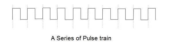
A Pulse signal is a unidirectional, non-sinusoidal signal which is similar to a square signal but it is not symmetrical like a square wave. A series of continuous pulse signals is simply called as a pulse train. A train of pulses indicate a sudden high level and a sudden low level transition from a baseline level which can be understood as ON/OFF respectively.
Hence a pulse signal indicates ON & OFF of the signal. If an electric switch is given a pulse input, it gets ON/OFF according to the pulse signal given. These switches which produce the pulse signals can be discussed later.
Terms Related to Pulse signals
There are few terms related to pulse signals which one should know. These can be understood with the help of the following figure.
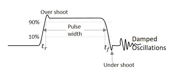
From the above figure,
Pulse width − Length of the pulse
Period of a waveform − Measurement from any point on one cycle to the same point on next cycle
Duty cycle − Ratio of the pulse width to the period
Rise time − Time it takes to rise from 10% to 90% of its maximum amplitude.
Fall time − Time signal takes to fall from 90% to 10% of its maximum amplitude.
Overshoot − Said to be occurred when leading edge of a waveform exceeds its normal maximum value.
Undershoot − Said to be occurred when trailing edge of a waveform exceeds its normal maximum value.
Ringing − Both undershoot and overshoot are followed by damped oscillations known as ringing.
The damped oscillations are the signal variations that indicate the decreasing amplitude and frequency of the signal which are of no use and unwanted. These oscillations are simple disturbances known as ringing.
In the next chapter, we will explain the concept of switching in electronics done using BJTs. We had already discussed switching using diodes in our ELECTRONIC CIRCUITS tutorial. Please refer.
Pulse Circuits - Switch
A Switch is a device that makes or breaks a circuit or a contact. As well, it can convert an analog data into digital data. The main requirements of a switch to be efficient are to be quick and to switch without sparking. The essential parts are a switch and its associated circuitry.
There are three types of Switches. They are −
- Mechanical switches
- Electromechanical switches or Relays
- Electronic switches
Mechanical Switches
The Mechanical Switches are the older type switches, which we previously used. But they had been replaced by Electro-mechanical switches and later on by electronic switches also in a few applications, so as to get over the disadvantages of the former.
The drawbacks of Mechanical Switches are as follows −
- They have high inertia which limits the speed of operation.
- They produce sparks while breaking the contact.
- Switch contacts are made heavy to carry larger currents.
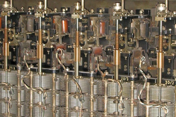
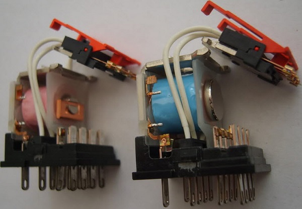
The mechanical switches look as in the figure below.
These mechanical switches were replaced by electro-mechanical switches or relays that have good speed of operation and reduce sparking.
Relays
Electromechanical switches are also called as Relays. These switches are partially mechanical and partially electronic or electrical. These are greater in size than electronic switches and lesser in size than mechanical switches.
Construction of a Relay
A Relay is made such that the making of contact supplies power to the load. In the external circuit, we have load power supply for the load and coil power supply for controlling the relay operation. Internally, a lever is connected to the iron yoke with a hard spring to hold the lever up. A Solenoid is connected to the yoke with an operating coil wounded around it. This coil is connected with the coil power supply as mentioned.
The figure below explains the construction and working of a Relay.
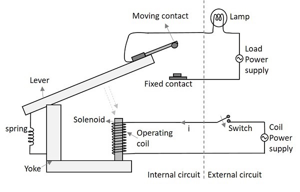
Working of a Relay
When the Switch is closed, an electrical path is established which energizes the solenoid. The lever is connected by a heavy spring which pulls up the lever and holds. The solenoid when gets energized, pulls the lever towards it, against the pulling force of the spring. When the lever gets pulled, the moving contact meets the fixed contact in order to connect the circuit. Thus the circuit connection is ON or established and the lamp glows indicating this.
When the switch is made OFF, the solenoid doesnt get any current and gets de-energized. This leaves the lever without any attraction towards the solenoid. The spring pulls the lever up, which breaks the contact. Thus the circuit connection gets switched OFF.
The figure below shows how a practical relay looks like.
Let us now have a look at the advantages and disadvantages of an Electro-magnetic switch.
Advantages
- A relay consumes less energy, even to handle a large power at the load.
- The operator can be at larger distance, even to handle high voltages.
- No Sparking while turning ON or OFF.
Disadvantages
- Slow in operation
- Parts are prone to wear and tear
Types of Latches in Relays
There are many kinds of relays depending upon their mode of operation such as Electromagnetic relay, solid-state relay, thermal relay, hybrid relay, reed relay etc.
The relay makes the connection with the help of a latch, as shown in the following figure.
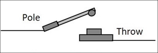
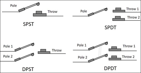
There are four types of latch connections in relays. They are −
Single Pole Single Throw (SPST) − This latch has a single pole and is thrown onto a single throw to make a connection.
Single Pole Double Throw (SPDT) − This latch has a single pole and double throw to make a connection. It has a choice to make connection with two different circuits for which two throws were connected.
Double Pole Single Throw (DPST) − This latch has a double pole and single throw to make a connection. Any of the two circuits can choose to make the connection with the circuit available at the single throw.
Double Pole Double Throw (DPDT) − This latch has a double pole and is thrown onto double throw to make two connections at the same time.
The following figure shows the diagrammatic view of all the four types of latch connections.
Electronic Switch
The next kind of switch to be discussed is the Electronic Switch. As mentioned earlier, transistor is the mostly used electronic switch for its high operating speed and absence of sparking.
The following image shows a practical electronic circuit built to make transistor work as a switch.
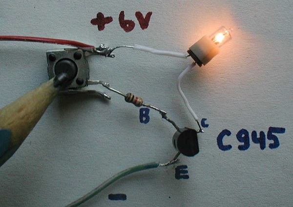
A Transistor works as a switch in ON condition, when it is operated in saturation region. It works as a switch in OFF condition, when it is operated in cut off region. It works as an amplifier in linear region, which lies between transistor and cut off. To have an idea regarding these regions of operation, refer to the transistors chapter from BASIC ELECTRONICS tutorial.
When the external conditions are so robust and high temperatures prevail, then a simple and normal transistor would not do. A special device named as Silicon Control Rectifier, simply SCR is used for such purposes. This will be discussed in detail, in the POWER ELECTRONICS tutorial.
Advantages of an Electronic Switch
There are many advantages of an Electronic switch such as
- Smaller in size
- Lighter in weight
- Sparkles operation
- No moving parts
- Less prone to wear and tear
- Noise less operation
- Faster operation
- Cheaper than other switches
- Less maintenance
- Troublefree service because of solid-state
A transistor is a simple electronic switch that has high operating speed. It is a solid state device and the contacts are all simple and hence the sparking is avoided while in operation. We will discuss the stages of switching operation in a transistor in the next chapter.
Pulse Circuits - Transistor as a Switch
A transistor is used as an electronic switch by driving it either in saturation or in cut off. The region between these two is the linear region. A transistor works as a linear amplifier in this region. The Saturation and Cut off states are important consideration in this regard.
ON & OFF States of a Transistor
There are two main regions in the operation of a transistor which we can consider as ON and OFF states. They are saturation and cut off states. Let us have a look at the behavior of a transistor in those two states.
Operation in Cut-off condition
The following figure shows a transistor in cut-off region.
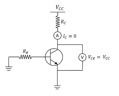
When the base of the transistor is given negative, the transistor goes to cut off state. There is no collector current. Hence IC = 0.
The voltage VCC applied at the collector, appears across the collector resistor RC. Therefore,
VCE = VCC
Operation in Saturation region
The following figure shows a transistor in saturation region.
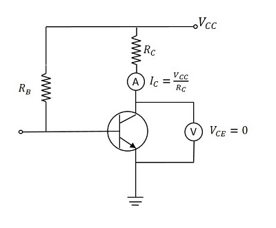
When the base voltage is positive and transistor goes into saturation, IC flows through RC.
Then VCC drops across RC. The output will be zero.
$$I_C = I_{C(sat)} \: = \: \frac{V_{CC}}{R_C} \: and \: V_{CE} = 0$$
Actually, this is the ideal condition. Practically, some leakage current flows. Hence we can understand that a transistor works as a switch when driven into saturation and cut off regions by applying positive and negative voltages to the base.
The following figure gives a better explanation.
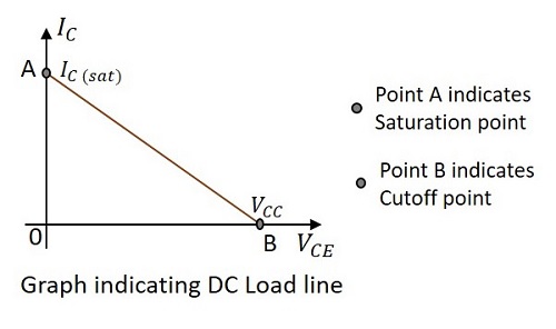
Observe the dc load line that connects the IC and VCC. If the transistor is driven into saturation, IC flows completely and VCE = 0 which is indicated by the point A.
If the transistor is driven into cut off, IC will be zero and VCE = VCC which is indicated by the point B. the line joining the saturation point A and cut off B is called as Load line. As the voltage applied here is dc, it is called as DC Load line.
Practical Considerations
Though the above-mentioned conditions are all convincing, there are a few practical limitations for such results to occur.
During the Cut off state
An ideal transistor has VCE = VCC and IC = 0.
But in practice, a smaller leakage current flows through the collector.
Hence IC will be a few μA.
This is called as Collector Leakage Current which is of course, negligible.
During the Saturation State
An ideal transistor has VCE = 0 and IC = IC(sat).
But in practice, VCE decreases to some value called knee voltage.
When VCE decreases more than knee voltage, β decreases sharply.
As IC = βIB this decreases the collector current.
Hence that maximum current IC which maintains VCE at knee voltage, is known as Saturation Collector Current.
Saturation Collector Current = $I_{C(sat)} \: = \: \frac{V_{CC} - V_{knee}}{R_C}$
A Transistor which is fabricated only to make it work for switching purposes is called as Switching Transistor. This works either in Saturation or in Cut off region. While in saturation state, the collector saturation current flows through the load and while in cut off state, the collector leakage current flows through the load.
Switching Action of a Transistor
A Transistor has three regions of operation. To understand the efficiency of operation, the practical losses are to be considered. So let us try to get an idea on how efficiently a transistor works as a switch.
During Cut off (OFF) state
The Base current IB = 0
The Collector current IC = ICEO (collector lekeage current)
Power Loss = Output Voltage × Output Current
$$= V_{CC} \times I_{CEO}$$
As ICEO is very small and VCC is also low, the loss will be of very low value. Hence, a transistor works as an efficient switch in OFF state.
During Saturation (ON) state
As discussed earlier,
$$I_{C(sat)} = \frac{V_{CC} - V_{knee}}{R_C}$$
The output voltage is Vknee.
Power loss = Output Voltage × Output Current
$$= \:V_{knee} \times I_{c(sat)}$$
As Vknee will be of small value, the loss is low. Hence, a transistor works as an efficient switch in ON state.
During Active region
The transistor lies between ON & OFF states. The transistor operates as a linear amplifier where small changes in input current cause large changes in the output current (ΔIC).
Switching Times
The Switching transistor has a pulse as an input and a pulse with few variations will be the output. There are a few terms that you should know regarding the timings of the switching output pulse. Let us go through them.
Let the input pulse duration = T
When the input pulse is applied the collector current takes some time to reach the steady state value, due to the stray capacitances. The following figure explains this concept.
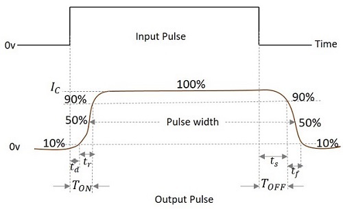
From the figure above,
Time delay(td) − The time taken by the collector current to reach from its initial value to 10% of its final value is called as the Time Delay.
Rise time(tr) − The time taken for the collector current to reach from 10% of its initial value to 90% of its final value is called as the Rise Time.
Turn-on time (TON) − The sum of time delay (td) and rise time (tr) is called as Turn-on time.
TON = td + tr
Storage time (ts) − The time interval between the trailing edge of the input pulse to the 90% of the maximum value of the output, is called as the Storage time.
Fall time (tf) − The time taken for the collector current to reach from 90% of its maximum value to 10% of its initial value is called as the Fall Time.
Turn-off time (TOFF) − The sum of storage time (ts) and fall time (tf) is defined as the Turn-off time.
TOFF = ts + tf
Pulse Width(W) − The time duration of the output pulse measured between two 50% levels of rising and falling waveform is defined as Pulse Width.
Pulse Circuits - Multivibrator Overview
A multivibrator circuit is nothing but a switching circuit. It generates non-sinusoidal waves such as Square waves, Rectangular waves and Saw tooth waves etc. Multivibrators are used as frequency generators, frequency dividers and generators of time delays and also as memory elements in computers etc.
A Transistor basically functions as an amplifier in its linear region. If a transistor amplifier output stage is joined with the previous amplifier stage, such a connection is said to be coupled. If a resistor is used in coupling two stages of such an amplifier circuit, it is called as Resistance coupled amplifier. For more details, refer to the AMPLIFIERS tutorial.
What is a Multivibrator?
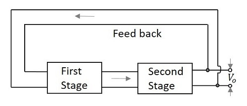
According to the definition, A Multivibrator is a two-stage resistance coupled amplifier with positive feedback from the output of one amplifier to the input of the other.
Two transistors are connected in feedback so that one controls the state of the other. Hence the ON and OFF states of the whole circuit, and the time periods for which the transistors are driven into saturation or cut off are controlled by the conditions of the circuit.
The following figure shows the block diagram of a Multivibrator.
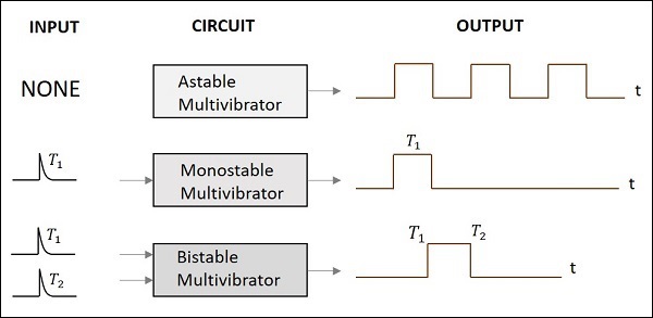
Types of Multivibrators
There are two possible states of a Multivibrator. In first stage, the transistor Q1 turns ON while the transistor Q2 turns OFF. In second stage, the transistor Q1 turns OFF while the transistor Q2 turns ON. These two states are interchanged for certain time periods depending upon the circuit conditions.
Depending upon the manner in which these two states are interchanged, the Multivibrators are classified into three types. They are
Astable Multivibrator
An Astable Multivibrator is such a circuit that it automatically switches between the two states continuously without the application of any external pulse for its operation. As this produces a continuous square wave output, it is called as a Free-running Multivibrator. The dc power source is a common requirement.
The time period of these states depends upon the time constants of the components used. As the Multivibrator keeps on switching, these states are known as quasi-stable or halfstable states. Hence there are two quasi-stable states for an Astable Multivibrator.
Monostable Multivibrator
A Monostable Multivibrator has a stable state and a quasi-stable state. This has a trigger input to one transistor. So, one transistor changes its state automatically, while the other one needs a trigger input to change its state.
As this Multivibrator produces a single output for each trigger pulse, this is known as One-shot Multivibrator. This Multivibrator cannot stay in quasi-stable state for a longer period while it stays in stable state until the trigger pulse is received.
Bistable Multivibrator
A Bistable Multivibrator has both the two states stable. It requires two trigger pulses to be applied to change the states. Until the trigger input is given, this Multivibrator cannot change its state. Its also known as flip-flop multivibrator.
As the trigger pulse sets or resets the output, and as some data, i.e., either high or low is stored until it is disturbed, this Multivibrator can be called as a Flip-flop. To know more about flip-flops, refer our DIGITAL CIRCUITS tutorial at: https://www.tutorialspoint.com/digital_circuits/index.htm
To get a clear idea on the above discussion, let us have a look at the following figure.
All these three Multivibrators are clearly discussed in the next chapters.
Pulse Circuits - Astable Multivibrator
An astable multivibrator has no stable states. Once the Multivibrator is ON, it just changes its states on its own after a certain time period which is determined by the RC time constants. A dc power supply or Vcc is given to the circuit for its operation.
Construction of Astable Multivibrator
Two transistors named Q1 and Q2 are connected in feedback to one another. The collector of transistor Q1 is connected to the base of transistor Q2 through the capacitor C1 and vice versa. The emitters of both the transistors are connected to the ground. The collector load resistors R1 and R4 and the biasing resistors R2 and R3 are of equal values. The capacitors C1 and C2 are of equal values.
The following figure shows the circuit diagram for Astable Multivibrator.
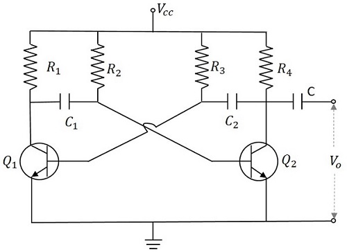
Operation of Astable Multivibrator
When Vcc is applied, the collector current of the transistors increase. As the collector current depends upon the base current,
$$I_c = \beta I_B$$
As no transistor characteristics are alike, one of the two transistors say Q1 has its collector current increase and thus conducts. The collector of Q1 is applied to the base of Q2 through C1. This connection lets the increased negative voltage at the collector of Q1 to get applied at the base of Q2 and its collector current decreases. This continuous action makes the collector current of Q2 to decrease further. This current when applied to the base of Q1 makes it more negative and with the cumulative actions Q1 gets into saturation and Q2 to cut off. Thus the output voltage of Q1 will be VCE (sat) and Q2 will be equal to VCC.
The capacitor C1 charges through R1 and when the voltage across C1 reaches 0.7v, this is enough to turn the transistor Q2 to saturation. As this voltage is applied to the base of Q2, it gets into saturation, decreasing its collector current. This reduction of voltage at point B is applied to the base of transistor Q1 through C2 which makes the Q1 reverse bias. A series of these actions turn the transistor Q1 to cut off and transistor Q2 to saturation. Now point A has the potential VCC. The capacitor C2 charges through R2. The voltage across this capacitor C2 when gets to 0.7v, turns on the transistor Q1 to saturation.
Hence the output voltage and the output waveform are formed by the alternate switching of the transistors Q1 and Q2. The time period of these ON/OFF states depends upon the values of biasing resistors and capacitors used, i.e., on the RC values used. As both the transistors are operated alternately, the output is a square waveform, with the peak amplitude of VCC.
Waveforms
The output waveforms at the collectors of Q1 and Q2 are shown in the following figures.
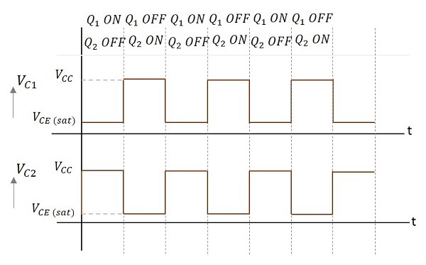
Frequency of Oscillations
The ON time of transistor Q1 or the OFF time of transistor Q2 is given by
t1 = 0.69R1C1
Similarly, the OFF time of transistor Q1 or ON time of transistor Q2 is given by
t2 = 0.69R2C2
Hence, total time period of square wave
t = t1 + t2 = 0.69(R1C1 + R2C2)
As R1 = R2 = R and C1 = C2 = C, the frequency of square wave will be
$$f = \frac{1}{t} = \frac{1}{1.38 R C} = \frac{0.7}{RC}$$
Advantages
The advantages of using an astable multivibrator are as follows −
- No external triggering required.
- Circuit design is simple
- Inexpensive
- Can function continuously
Disadvantages
The drawbacks of using an astable multivibrator are as follows −
- Energy absorption is more within the circuit.
- Output signal is of low energy.
- Duty cycle less than or equal to 50% cant be achieved.
Applications
Astable Multivibrators are used in many applications such as amateur radio equipment, Morse code generators, timer circuits, analog circuits, and TV systems.
Pulse Circuits - Monostable Multivibrator
A monostable multivibrator, as the name implies, has only one stable state. When the transistor conducts, the other remains in non-conducting state. A stable state is such a state where the transistor remains without being altered, unless disturbed by some external trigger pulse. As Monostable works on the same principle, it has another name called as One-shot Multivibrator.
Construction of Monostable Multivibrator
Two transistors Q1 and Q2 are connected in feedback to one another. The collector of transistor Q1 is connected to the base of transistor Q2 through the capacitor C1. The base Q1 is connected to the collector of Q2 through the resistor R2 and capacitor C. Another dc supply voltage VBB is given to the base of transistor Q1 through the resistor R3. The trigger pulse is given to the base of Q1 through the capacitor C2 to change its state. RL1 and RL2 are the load resistors of Q1 and Q2.
One of the transistors, when gets into a stable state, an external trigger pulse is given to change its state. After changing its state, the transistor remains in this quasi-stable state or Meta-stable state for a specific time period, which is determined by the values of RC time constants and gets back to the previous stable state.
The following figure shows the circuit diagram of a Monostable Multivibrator.
Operation of Monostable Multivibrator
Firstly, when the circuit is switched ON, transistor Q1 will be in OFF state and Q2 will be in ON state. This is the stable state. As Q1 is OFF, the collector voltage will be VCC at point A and hence C1 gets charged. A positive trigger pulse applied at the base of the transistor Q1 turns the transistor ON. This decreases the collector voltage, which turns OFF the transistor Q2. The capacitor C1 starts discharging at this point of time. As the positive voltage from the collector of transistor Q2 gets applied to transistor Q1, it remains in ON state. This is the quasi-stable state or Meta-stable state.
The transistor Q2 remains in OFF state, until the capacitor C1 discharges completely. After this, the transistor Q2 turns ON with the voltage applied through the capacitor discharge. This turn ON the transistor Q1, which is the previous stable state.
Output Waveforms
The output waveforms at the collectors of Q1 and Q2 along with the trigger input given at the base of Q1 are shown in the following figures.
The width of this output pulse depends upon the RC time constant. Hence it depends on the values of R1C1. The duration of pulse is given by
$$T = 0.69R_1 C_1$$
The trigger input given will be of very short duration, just to initiate the action. This triggers the circuit to change its state from Stable state to Quasi-stable or Meta-stable or Semi-stable state, in which the circuit remains for a short duration. There will be one output pulse for one trigger pulse.
Advantages
The advantages of Monostable Multivibrator are as follows −
- One trigger pulse is enough.
- Circuit design is simple
- Inexpensive
Disadvantages
The major drawback of using a monostable multivibrator is that the time between the applications of trigger pulse T has to be greater than the RC time constant of the circuit.
Applications
Monostable Multivibrators are used in applications such as television circuits and control system circuits.
Pulse Circuits - Bistable Multivibrator
A Bistable Multivibrator has two stable states. The circuit stays in any one of the two stable states. It continues in that state, unless an external trigger pulse is given. This Multivibrator is also known as Flip-flop. This circuit is simply called as Binary.
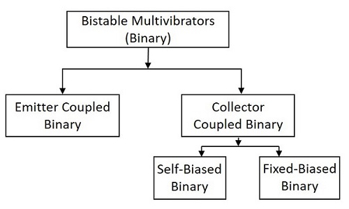
There are few types in Bistable Multivibrators. They are as shown in the following figure.
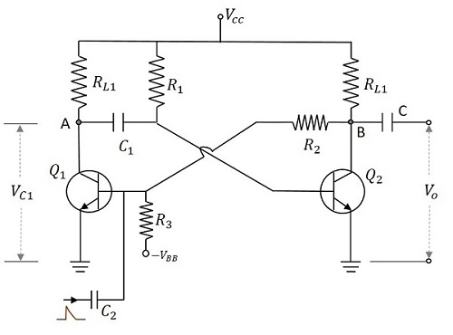
Construction of Bistable Multivibrator
Two similar transistors Q1 and Q2 with load resistors RL1 and RL2 are connected in feedback to one another. The base resistors R3 and R4 are joined to a common source VBB. The feedback resistors R1 and R2 are shunted by capacitors C1 and C2 known as Commutating Capacitors. The transistor Q1 is given a trigger input at the base through the capacitor C3 and the transistor Q2 is given a trigger input at its base through the capacitor C4.
The capacitors C1 and C2 are also known as Speed-up Capacitors, as they reduce the transition time, which means the time taken for the transfer of conduction from one transistor to the other.
The following figure shows the circuit diagram of a self-biased Bistable Multivibrator.
Operation of Bistable Multivibrator
When the circuit is switched ON, due to some circuit imbalances as in Astable, one of the transistors, say Q1 gets switched ON, while the transistor Q2 gets switched OFF. This is a stable state of the Bistable Multivibrator.
By applying a negative trigger at the base of transistor Q1 or by applying a positive trigger pulse at the base of transistor Q2, this stable state is unaltered. So, let us understand this by considering a negative pulse at the base of transistor Q1. As a result, the collector voltage increases, which forward biases the transistor Q2. The collector current of Q2 as applied at the base of Q1, reverse biases Q1 and this cumulative action, makes the transistor Q1 OFF and transistor Q2 ON. This is another stable state of the Multivibrator.
Now, if this stable state has to be changed again, then either a negative trigger pulse at transistor Q2 or a positive trigger pulse at transistor Q1 is applied.
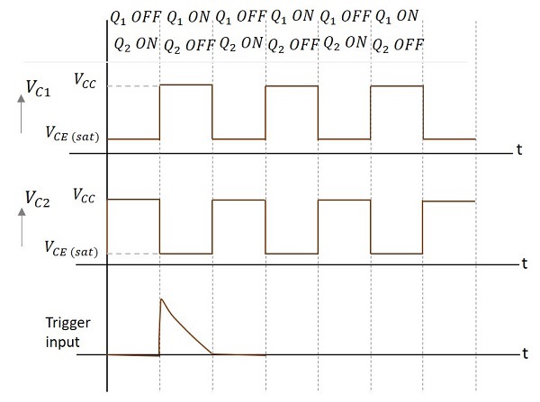
Output Waveforms
The output waveforms at the collectors of Q1 and Q2 along with the trigger inputs given at the bases of QW and Q2 are shown in the following figures.
Advantages
The advantages of using a Bistable Multivibrator are as follows −
- Stores the previous output unless disturbed.
- Circuit design is simple
Disadvantages
The drawbacks of a Bistable Multivibrator are as follows −
- Two kinds of trigger pulses are required.
- A bit costlier than other Multivibrators.
Applications
Bistable Multivibrators are used in applications such as pulse generation and digital operations like counting and storing of binary information.
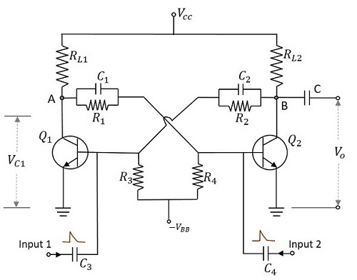
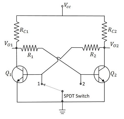
Fixed-bias Binary
A fixed-bias binary circuit is similar to an Astable Multivibrator but with a simple SPDT switch. Two transistors are connected in feedback with two resistors, having one collector connected to the base of the other. The figure below shows the circuit diagram of a fixed-bias binary.
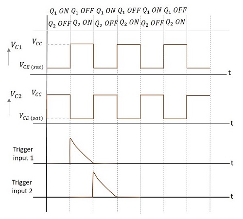
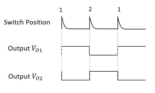
To understand the operation, let us consider the switch to be in position 1. Now the transistor Q1 will be OFF as the base is grounded. The collector voltage at the output terminal VO1 will be equal to VCC which turns the transistor Q2 ON. The output at the terminal VO2 goes LOW. This is a stable state which can be altered only by an external trigger. The change of switch to position 2, works as a trigger.
When the switch is altered, the base of transistor Q2 is grounded turning it to OFF state. The collector voltage at VO2 will be equal to VCC which is applied to transistor Q1 to turn it ON. This is the other stable state. The triggering is achieved in this circuit with the help of a SPDT Switch.
There are two main types of triggering given to the binary circuits. They are
- Symmetrical Triggering
- Asymmetrical Triggering
Schmitt Trigger
Another type of binary circuit which is ought to be discussed is the Emitter Coupled Binary Circuit. This circuit is also called as Schmitt Trigger circuit. This circuit is considered as a special type of its kind for its applications.
The main difference in the construction of this circuit is that the coupling from the output C2 of the second transistor to the base B1 of the first transistor is missing and that feedback is obtained now through the resistor Re. This circuit is called as the Regenerative circuit for this has a positive feedback and no Phase inversion. The circuit of Schmitt trigger using BJT is as shown below.
Initially we have Q1 OFF and Q2 ON. The voltage applied at the base of Q2 is VCC through RC1 and R1. So the output voltage will be
$$V_0 = V_{CC} - (I_{C2}R_{c2})$$
As Q2 is ON, there will be a voltage drop across RE, which will be (IC2 + IB2) RE. Now this voltage gets applied at the emitter of Q1. The input voltage is increased and until Q1 reaches cut-in voltage to turn ON, the output remains LOW. With Q1 ON, the output will increase as Q2 is also ON. As the input voltage continues to rise, the voltage at the points C1 and B2 continue to fall and E2 continues to rise. At certain value of the input voltage, Q2 turns OFF. The output voltage at this point will be VCC and remains constant though the input voltage is further increased.
As the input voltage rises, the output remains LOW until the input voltage reaches V1 where
$$V_1 = [V_{CC} - (I_{C2}R_{C2})]$$
The value where the input voltage equals V1, lets the transistor Q1 to enter into saturation, is called UTP (Upper Trigger Point). If the voltage is already greater than V1, then it remains there until the input voltage reaches V2, which is a low level transition. Hence the value for which input voltage will be V2 at which Q2 gets into ON condition, is termed as LTP (Lower Trigger Point).
Output Waveforms
The output waveforms are obtained as shown below.
The Schmitt trigger circuit works as a Comparator and hence compares the input voltage with two different voltage levels called as UTP (Upper Trigger Point) and LTP (Lower Trigger Point). If the input crosses this UTP, it is considered as a HIGH and if it gets below this LTP, it is taken as a LOW. The output will be a binary signal indicating 1 for HIGH and 0 for LOW. Hence an analog signal is converted into a digital signal. If the input is at intermediate value (between HIGH and LOW) then the previous value will be the output.
This concept depends upon the phenomenon called as Hysteresis. The transfer characteristics of electronic circuits exhibit a loop called as Hysteresis. It explains that the output values depends upon both the present and the past values of the input. This prevents unwanted frequency switching in Schmitt trigger circuits
Advantages
The advantages of Schmitt trigger circuit are
- Perfect logic levels are maintained.
- It helps avoiding Meta-stability.
- Preferred over normal comparators for its pulse conditioning.
Disadvantages
The main disadvantages of a Schmitt trigger are
- If the input is slow, the output will be slower.
- If the input is noisy, the output will be noisier.
Applications of Schmitt trigger
Schmitt trigger circuits are used as Amplitude Comparator and Squaring Circuit. They are also used in Pulse conditioning and sharpening circuits.
These are the Multivibrator circuits using transistors. The same Multivibrators are designed using operational amplifiers and also IC 555 timer circuits, which are discussed in further tutorials.
Time Base Generators Overview
After having discussed the fundamentals of pulse circuits, let us now go through different circuits that generate and deal with Saw tooth waves. A Saw tooth wave increases linearly with time and has a sudden decrease. This is also called as a Time base signal. Actually, this is the ideal output of a time base generator.
What is a Time Base Generator?
An Electronic generator that generates the high frequency saw tooth waves can be termed as a Time Base Generator. It can also be understood as an electronic circuit which generates an output voltage or current waveform, a portion of which varies linearly with time. The horizontal velocity of a time base generator must be constant.
To display the variations of a signal with respect to time on an oscilloscope, a voltage that varies linearly with time, has to be applied to the deflection plates. This makes the signal to sweep the beam horizontally across the screen. Hence the voltage is called as Sweep Voltage. The Time Base Generators are called as Sweep Circuits.
Features of a Time Base Signal
To generate a time base waveform in a CRO or a picture tube, the deflecting voltage increases linearly with time. Generally, a time base generator is used where the beam deflects over the screen linearly and returns to its starting point. This occurs during the process of Scanning. A cathode ray tube and also a picture tube works on the same principle. The beam deflects over the screen from one side to the other (generally from left to right) and gets back to the same point.
This phenomenon is termed as Trace and Retrace. The deflection of beam over the screen from left to right is called as Trace, while the return of the beam from right to left is called as Retrace or Fly back. Usually this retrace is not visible. This process is done with the help of a saw tooth wave generator which sets the time period of the deflection with the help of RC components used.
Let us try to understand the parts of a saw-tooth wave.
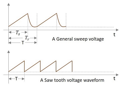
In the above signal, the time during which the output increases linearly is called as Sweep Time (TS) and the time taken for the signal to get back to its initial value is called as Restoration Time or Fly back Time or Retrace Time (Tr). Both of these time periods together form the Time period of one cycle of the Time base signal.
Actually, this Sweep voltage waveform we get is the practical output of a sweep circuit whereas the ideal output has to be the saw tooth waveform shown in the above figure.
Types of Time base Generators
There are two types of Time base Generators. They are −
Voltage Time Base Generators − A time base generator that provides an output voltage waveform that varies linearly with time is called as a Voltage Time base Generator.
Current Time Base Generator − A time base generator that provides an output current waveform that varies linearly with time is called as a Current Time base Generator.
Applications
Time Base Generators are used in CROs, televisions, RADAR displays, precise time measurement systems, and time modulation.
Errors of Sweep Signals
After generating the sweep signals, it is time to transmit them. The transmitted signal may be subjected to deviation from linearity. To understand and correct the errors occurred, we must have some knowledge on the common errors that occur.
The deviation from linearity is expressed in three different ways. They are −
- The Slope or Sweep Speed Error
- The Displacement Error
- The Transmission Error
Let us discuss these in detail.
The Slope or Sweep Speed Error (es)
A Sweep voltage must increase linearly with time. The rate of change of sweep voltage with time must be constant. This deviation from linearity is defined as Slope Speed Error or Sweep Speed Error.
Slope or Sweep speed eror es = $\frac{difference \: in\: slope\: at \: the\: beginning\: and\: end\: of\: sweep}{initial \: value \:of \: slope}$
$$= \frac{\left (\frac{\mathrm{d} V_0}{\mathrm{d} t} \right )_{t = 0} - \left( \frac{\mathrm{d} V_0}{\mathrm{d} t} \right)_{t = T_s}}{\left( \frac{\mathrm{d} V_0}{\mathrm{d} t}\right )_{t = 0}}$$
The Displacement Error (ed)
An important criterion of linearity is the maximum difference between the actual sweep voltage and the linear sweep which passes through the beginning and end points of the actual sweep.
This can be understood from the following figure.
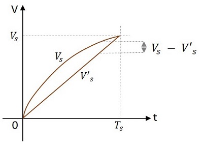
The displacement error ed is defined as
ed = $\frac{(actual\: speed)\thicksim (linear\: sweep \: that\: passes\: beginning \: and \: ending\: of\: actual\: sweep)}{amplitude\: of\: sweep\: at\: the \: end\: of\: sweep\: time}$
$$= \: \frac{(V_s - V_s)_{max}}{V_s}$$
Where Vs is the actual sweep and Vs is the linear sweep.
The Transmission Error (et)
When a sweep signal passes through a high pass circuit, the output gets deviated from the input as shown below.
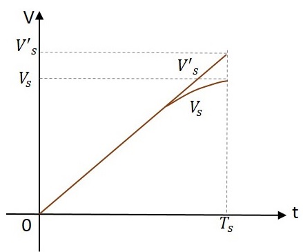
This deviation is expressed as transmission error.
Transmission Error = $\frac{(input)\: \thicksim \:(output)}{input\: at \: the\: end\: of\: the\: sweep}$
$$e_t = \frac{V_s V}{V_s}$$
Where Vs is the input and Vs is the output at the end of the sweep i.e. at t = Ts.
If the deviation from linearity is very small and the sweep voltage may be approximated by the sum of linear and quadratic terms in t, then the above three errors are related as
$$e_d = \frac{e_s}{8} = \frac{e_t}{4}$$
$$e_s = 2e_t = 8e_d$$
The sweep speed error is more dominant than the displacement error.
Types of Time Base Generators
As we have an idea that there are two types of time base generators, let us try to know about the basic circuits of those time base generator circuits.
Voltage Time base Generator
A time base generator that provides an output voltage waveform that varies linearly with time is called as a Voltage Time base Generator.
Let us try to understand the basic voltage time base generator.
A Simple Voltage Time base Generator
A basic simple RC time base generator or a Ramp generator or a sweep circuit consists of a capacitor C which charges through VCC via a series connected resistor R2. It contains a BJT whose base is connected through the resistor R1. The capacitor charges through the resistor and discharges through the transistor.
The following figure shows a simple RC sweep circuit.
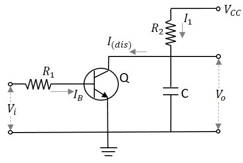
By the application of a positive going voltage pulse, the transistor Q turns ON to saturation and the capacitor rapidly discharges through Q and R1 to VCE (sat). When the input pulse ends, Q switches OFF and the capacitor C starts charging and continues to charge until the next input pulse. This process repeats as shown in the waveform below.
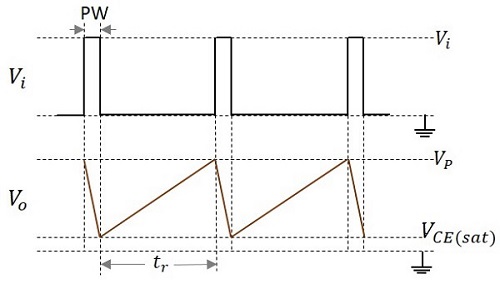
When the transistor turns ON it provides a low resistance path for the capacitor to discharge quickly. When the transistor is in OFF condition, the capacitor will charge exponentially to the supply voltage VCC, according to the equation
$$V_0 = V_{CC}[1 - exp(-t/RC)]$$
Where
- VO = instantaneous voltage across the capacitor at time t
- VCC = supply voltage
- t = time taken
- R = value of series resistor
- C = value of the capacitor
Let us now try to know about different types of time base generators.
The circuit just we had discussed, is a voltage time base generator circuit as it offers the output in the form of voltage.
Current Time base Generator
A time base generator that provides an output current waveform that varies linearly with time is called as a Current Time base Generator.
Let us try to understand the basic current time base generator.
A Simple Current Time base Generator
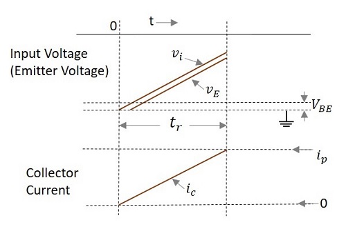
A basic simple RC time base generator or a Ramp generator or a sweep circuit consists of a common-base configuration transistor and two resistors, having one in emitter and another in collector. The VCC is given to the collector of the transistor. The circuit diagram of a basic ramp current generator is as shown here under.
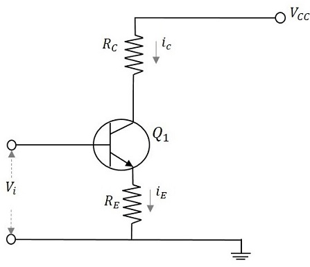
A transistor connected in common-base configuration has its collector current vary linearly with its emitter current. When the emitter current is held constant, the collector current also will be near constant value, except for very smaller values of collector base voltages.
As the input voltage Vi is applied at the base of the transistor, it appears at the emitter which produces the emitter current iE and this increases linearly as Vi increase from zero to its peak value. The collector current increases as the emitter current increases, because iC is closely equal to iE.
The instantaneous value of load current is
$$i_L i_C \thickapprox (v_i - V_{BE})/R_E$$
The input and output waveforms are as shown below.
Bootstrap Time Base Generator
A bootstrap sweep generator is a time base generator circuit whose output is fed back to the input through the feedback. This will increase or decrease the input impedance of the circuit. This process of bootstrapping is used to achieve constant charging current.
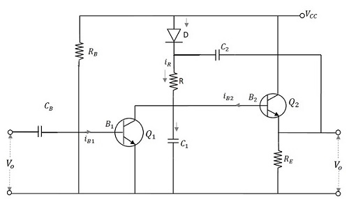
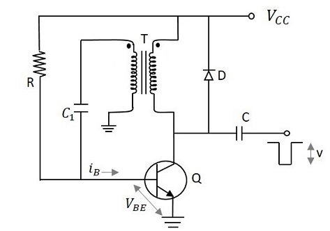
Construction of Bootstrap Time Base Generator
The boot strap time base generator circuit consists of two transistors, Q1 which acts as a switch and Q2 which acts as an emitter follower. The transistor Q1 is connected using an input capacitor CB at its base and a resistor RB through VCC. The collector of the transistor Q1 is connected to the base of the transistor Q2. The collector of Q2 is connected to VCC while its emitter is provided with a resistor RE across which the output is taken.
A diode D is taken whose anode is connected to VCC while cathode is connected to the capacitor C2 which is connected to the output. The cathode of diode D is also connected to a resistor R which is in turn connected to a capacitor C1. This C1 and R are connected through the base of Q2 and collector of Q1. The voltage that appears across the capacitor C1 provides the output voltage Vo.
The following figure explains the construction of the boot strap time base generator.
Operation of Bootstrap Time Base Generator
Before the application of gating waveform at t = 0, as the transistor gets enough base drive from VCC through RB, Q1 is ON and Q2 is OFF. The capacitor C2 charges to VCC through the diode D. Then a negative trigger pulse from the gating waveform of a Monostable Multivibrator is applied at the base of Q1 which turns Q1 OFF. The capacitor C2 now discharges and the capacitor C1 charges through the resistor R. As the capacitor C2 has large value of capacitance, its voltage levels (charge and discharge) vary at a slower rate. Hence it discharges slowly and maintains a nearly constant value during the ramp generation at the output of Q2.
During the ramp time, the diode D is reverse biased. The capacitor C2 provides a small current IC1 for the capacitor C1 to charge. As the capacitance value is high, though it provides current, it doesnt make much difference in its charge. When Q1 gets ON at the end of ramp time, C1 discharges rapidly to its initial value. This voltage appears across VO. Consequently, the diode D gets forward biased again and the capacitor C2 gets a pulse of current to recover its small charge lost during the charging of C1. Now, the circuit is ready to produce another ramp output.
The capacitor C2 which helps in providing some feedback current to the capacitor C1 acts as a boot strapping capacitor that provides constant current.
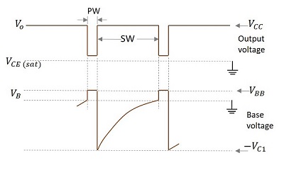
Output Waveforms
The output waveforms are obtained as shown in the following figure.
The pulse given at the input and the voltage VC1 which denotes the charging and discharging of the capacitor C1 which contributes the output are shown in the figure above.
Advantage
The main advantage of this boot strap ramp generator is that the output voltage ramp is very linear and the ramp amplitude reaches the supply voltage level.
Pulse Circuits - Miller Sweep Generator
The transistor Miller time base generator circuit is the popular Miller integrator circuit that produces a sweep waveform. This is mostly used in horizontal deflection circuits.
Let us try to understand the construction and working of a Miller time base generator circuit.
Construction of Miller Sweep Generator
The Miller time base generator circuit consists of a switch and a timing circuit in the initial stage, whose input is taken from the Schmitt gate generator circuit. The amplifier section is the following one which has three stages, first being an emitter follower, second an amplifier and the third one is also an emitter follower.
An emitter follower circuit usually acts as a Buffer amplifier. It has a low output impedance and a high input impedance. The low output impedance lets the circuit drive a heavy load. The high input impedance keeps the circuit from not loading its previous circuit. The last emitter follower section will not load the previous amplifier section. Because of this, the amplifier gain will be high.
The capacitor C placed between the base of Q1 and the emitter of Q3 is the timing capacitor. The values of R and C and the variation in the voltage level of VBB changes the sweep speed. The figure below shows the circuit of a Miller time base generator.
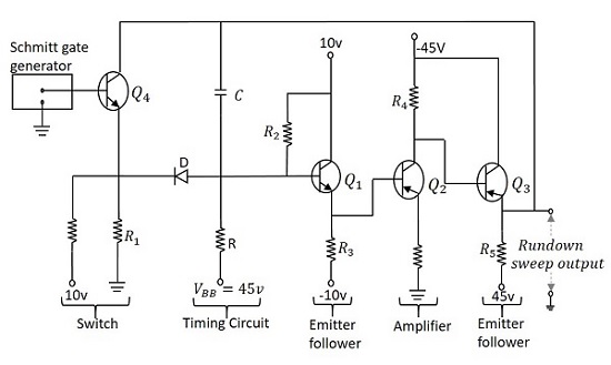
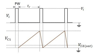
Operation of Miller Sweep Generator
When the output of Schmitt trigger generator is a negative pulse, the transistor Q4 turns ON and the emitter current flows through R1. The emitter is at negative potential and the same is applied at the cathode of the diode D, which makes it forward biased. As the capacitor C is bypassed here, it is not charged.
The application of a trigger pulse, makes the Schmitt gate output high, which in turn, turns the transistor Q4 OFF. Now, a voltage of 10v is applied at the emitter of Q4 that makes the current flow through R1 which also makes the diode D reverse biased. As the transistor Q4 is in cutoff, the capacitor C gets charged from VBB through R and provides a rundown sweep output at the emitter of Q3. The capacitor C discharges through D and transistor Q4 at the end of the sweep.
Considering the effect of capacitance C1, the slope speed or sweep speed error is given by
$$e_s = \frac{V_s}{V} \left( 1- A + \frac{R}{R_i} + \frac{C}{C_i} \right )$$
Applications
Miller sweep circuits are the most commonly used integrator circuit in many devices. It is a widely used saw tooth generator.
Pulse Circuits - Unijunction Transistor
Unijunction Transistor is such a transistor that has a single PN junction, but still not a diode. Unijunction Transistor, or simply UJT has an emitter and two bases, unlike a normal transistor. This component is especially famous for its negative resistance property and also for its application as a relaxation oscillator.
Construction of UJT
A bar of highly resistive n-type silicon, is considered to form the base structure. Two Ohmic contacts are drawn at both the ends being both the bases. An aluminum rod like structure is attached to it which becomes the emitter. This emitter lies near to the base 2 and a bit far to the base1. Both of these join to form a PN junction. As single PN junction is present, this component is called as a Unijunction transistor.
An internal resistance called as intrinsic resistance is present inside the bar whose resistance value depends upon the doping concentration of the bar. The construction and symbol of UJT are as shown below.
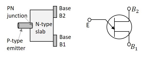
In the symbol, the emitter is indicated by an inclined arrow and the remaining two ends indicate the bases. As the UJT is understood as a combination of diode and some resistance, the internal structure of UJT can be indicated by an equivalent diagram to explain the working of UJT.
Working of UJT
The working of UJT can be understood by its equivalent circuit. The voltage applied at the emitter is indicated as VE and the internal resistances are indicated as RB1 and RB2 at bases 1 and 2 respectively. Both resistances present internally are together called as intrinsic resistance, indicated as RBB. The voltage across RB1 can be denoted as V1. The dc voltage applied for the circuit to function is VBB.
The UJT equivalent circuit is as given below.
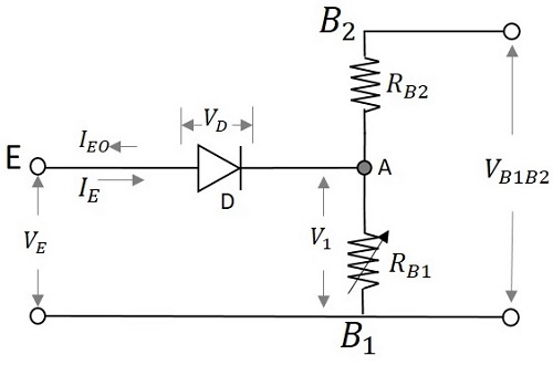
Initially when no voltage is applied,
$$V_E = 0$$
Then the voltage VBB is applied through RB2. The diode D will be in reverse bias. The voltage across the diode will be VB which is the barrier voltage of the emitter diode. Due to the application of VBB, some voltage appears at point A. So, the total voltage will be VA + VB.
Now if the emitter voltage VE is increased, the current IE flows through the diode D. This current makes the diode forward biased. The carriers get induced and the resistance RB1 goes on decreasing. Therefore, the potential across RB1 which means VB1 also decreases.
$$V_{B1} = \left( \frac{R_{B1}}{R_{B1} + R_{B2}} \right )V_{BB}$$
As VBB is constant and RB1 decreases to its minimum value due to the doping concentration of the channel, VB1 also decreases.
Actually, the resistances present internally are together called as intrinsic resistance, indicated as RBB. The resistance mentioned above can be indicated as
$$R_{BB} = R_{B1} + R_{B2}$$
$$\left( \frac{R_{B1}}{R_{BB}} \right ) = \eta$$
The symbol η is used to represent the total resistance applied.
Hence voltage across VB1 is represented as
$$V_{B1} = \eta V_{BB}$$
The emitter voltage is given as
$$V_E = V_D + V_{B1}$$
$$V_E = 0.7 + V_{B1}$$
Where VD is the voltage across the diode.
As the diode gets forward biased, the voltage across it will be 0.7v. So, this is constant and VB1 goes on decreasing. Hence VE goes on decreasing. It decreases to a least value which may be denoted VV called as Valley voltage. The voltage at which the UJT gets switched ON is the Peak Voltage denoted as VP.
V-I Characteristics of UJT
The concept discussed till now is clearly understood from the following graph shown below.
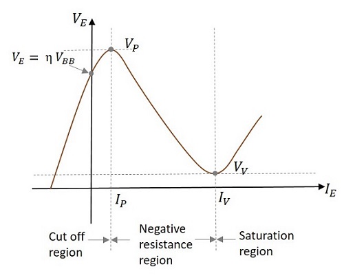
Initially when VE is zero, some reverse current IE flows until, the value of VE reaches a point at which
$$V_E = \eta V_{BB}$$
This is the point where the curve touches the Y-axis.
When VE reaches a voltage where
$$V_E = \eta V_{BB} + V_D$$
At this point, the diode gets forward biased.
The voltage at this point is called as VP (Peak Voltage) and the current at this point is called as IP (Peak Current). The portion in the graph till now, is termed as Cut off region as the UJT was in OFF state.
Now, when VE is further increased, the resistance RB1 and then the voltage V1 also decreases, but the current through it increases. This is the Negative resistance property and hence this region is called as Negative resistance region.
Now, the voltage VE reaches a certain point where further increase leads to the increase in voltage across RB1. The voltage at this point is called as VV (Valley Voltage) and the current at this point is called as IV (Valley Current). The region after this is termed as Saturation region.
Applications of UJT
UJTs are most prominently used as relaxation oscillators. They are also used in Phase Control Circuits. In addition, UJTs are widely used to provide clock for digital circuits, timing control for various devices, controlled firing in thyristors, and sync pulsed for horizontal deflection circuits in CRO.
UJT as Relaxation Oscillator
An oscillator is a device that produces a waveform by its own, without any input. Though some dc voltage is applied for the device to work, it will not produce any waveform as input. A relaxation oscillator is a device that produces a non-sinusoidal waveform on its own. This waveform depends generally upon the charging and discharging time constants of a capacitor in the circuit.
Construction and Working
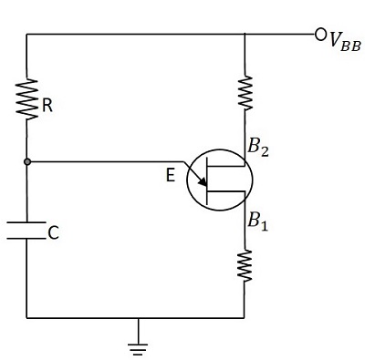
The emitter of UJT is connected with a resistor and capacitor as shown. The RC time constant determines the timings of the output waveform of the relaxation oscillator. Both the bases are connected with a resistor each. The dc voltage supply VBB is given.
The following figure shows how to use a UJT as a relaxation oscillator.
Initially, the voltage across the capacitor is zero.
$$V_c = 0$$
The UJT is in OFF condition. The resistor R provides a path for the capacitor C to charge through the voltage applied.
The capacitor charges according to the voltage
$$V = V_0(1 - e^{-t/RC})$$
The capacitor usually starts charging and continues to charge until the maximum voltage VBB. But in this circuit, when the voltage across capacitor reaches a value, which enables the UJT to turn ON (the peak voltage) then the capacitor stops to charge and starts discharging through UJT. Now, this discharging continues until the minimum voltage which turns the UJT OFF (the valley voltage). This process continues and the voltage across the capacitor, when indicated on a graph, the following waveform is observed.
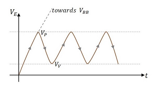
So, the charge and discharge of capacitor produces the sweep waveform as shown above. The charging time produces increasing sweep and the discharging time produces decreasing sweep. The repetition of this cycle, forms a continuous sweep output waveform.
As the output is a non-sinusoidal waveform, this circuit is said to be working as a relaxation oscillator.
Applications of Relaxation Oscillator
Relaxation oscillators are widely used in function generators, electronic beepers, SMPS, inverters, blinkers, and voltage controlled oscillators.
Pulse Circuits - Synchronization
In any system, having different waveform generators, all of them are required to be operated in synchronism. Synchronization is the process of making two or more waveform generators arrive at some reference point in the cycle exactly at the same time.
Types of Synchronization
Synchronization can be of the following two types −
One-to-one basis
All the generators are operated at a same frequency.
All of them arrive at some reference point in the cycle exactly at the same time.
Sync with frequency division
Generators operate at different frequency which are integral multiples of each other.
All of them arrive at some reference point in the cycle exactly at the same time.
Relaxation devices
Relaxation circuits are the circuits in which the timing interval is established through the gradual charging of a capacitor, the timing interval being terminated by the sudden discharge (relaxation) of a capacitor.
Examples − Multivibrators, sweep circuits, blocking oscillators, etc.
We have observed in the UJT relaxation oscillator circuit that the capacitor stops charging when the negative resistance device such as UJT turns ON. The capacitor then discharges through it to reach its minimum value. Both these points denote the maximum and minimum voltage points of a sweep waveform.
Synchronization in Relaxation Devices
If the high voltage or peak voltage or breakdown voltage of the sweep waveform has to be brought down to a lower level, then an external signal can be applied. This signal to be applied is the synchronized signal whose effect lowers the voltage of peak or breakdown voltage, for the duration of the pulse. A synchronizing pulse is generally applied at the emitter or at the base of a negative resistance device. A pulse train having regularly spaced pulses is applied to achieve synchronization.
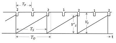
Though the synchronizing signal is applied first few pulses will have no effect on the sweep generator as the amplitude of the sweep signal at the occurrence of the pulse, in addition with the amplitude of the pulse is less than VP. Hence the sweep generator runs unsynchronized. The exact moment at which UJT turns ON is determined by the instant ofoccurrence of a pulse. This is the point where the sync signal achieves synchronization with the sweep signal. This can be observed from the following figure.
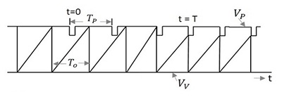
Where,
- TP is the time period of the pulse signal
- TO is the time period of the sweep signal
- VP is the Peak or breakdown voltage
- VV is the Valley or Maintaining voltage
To achieve synchronization, the pulse timing interval TP should be less than the time period of sweep generator TO, so that it terminates the sweep cycle prematurely. The synchronization cannot be achieved if the pulse timing interval TP is greater than the time period of sweep generator TO and also if the amplitude of the pulses is not large enough to bridge the gap between the quiescent breakdown and the sweep voltage, though TP is less than TO.
Frequency Division in Sweep Circuits
In the previous topic, we have observed that synchronization gets achieved when the following conditions are satisfied. They are
When TP < TO
When the amplitude of the pulse is sufficient to terminate each cycle prematurely.
Satisfying these two conditions, though synchronization is achieved, we may often come across a certain interesting pattern in the sweep with regard to sync timing. The following figure illustrates this point.
We can observe that the amplitude VS of the sweep after synchronization is less than the unsynchronized amplitude VS. Also the time period TO of the sweep is adjusted according to the time period of the pulse but leaving a cycle in-between. Which means, one sweep cycle is made equal to two pulse cycles. The synchronization is achieved for every alternate cycle, which states
$$T_o > 2T_P$$
The sweep timing TO be restricted to TS and its amplitude is reduced to VS.
As every second pulse is made in synchronism with the sweep cycle, this signal can be understood as a circuit that exhibits frequency division by a factor of 2. Hence the frequency division circuit is obtained by synchronization.
Pulse Circuits - Blocking Oscillators
An oscillator is a circuit that provides an alternating voltage or current by its own, without any input applied. An Oscillator needs an amplifier and also a feedback from the output. The feedback provided should be regenerative feedback which along with the portion of the output signal, contains a component in the output signal, which is in phase with the input signal. An oscillator that uses a regenerative feedback to generate a nonsinusoidal output is called as Relaxation Oscillator.
We have already seen UJT relaxation oscillator. Another type of relaxation oscillator is the Blocking oscillator.
Blocking Oscillator
A blocking oscillator is a waveform generator that is used to produce narrow pulses or trigger pulses. While having the feedback from the output signal, it blocks the feedback, after a cycle, for certain predetermined time. This feature of blocking the output while being an oscillator, gets the name blocking oscillator to it.
In the construction of a blocking oscillator, the transistor is used as an amplifier and the transformer is used for feedback. The transformer used here is a Pulse transformer. The symbol of a pulse transformer is as shown below.
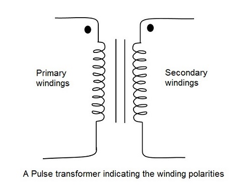
Pulse Transformer
A Pulse transformer is one which couples a source of rectangular pulses of electrical energy to the load. Keeping the shape and other properties of pulses unchanged. They are wide band transformers with minimum attenuation and zero or minimum phase change.
The output of the transformer depends upon the charge and discharge of the capacitor connected.
The regenerative feedback is made easy by using pulse transformer. The output can be fed back to the input in the same phase by properly choosing the winding polarities of the pulse transformer. Blocking oscillator is such a free-running oscillator made using a capacitor and a pulse transformer along with a single transistor which is cut off for most of the duty cycle producing periodic pulses.
Using the blocking oscillator, Astable and Monostable operations are possible. But Bistable operation is not possible. Let us go through them.
Monostable Blocking Oscillator
If the blocking oscillator needs a single pulse, to change its state, it is called as a Monostable blocking oscillator circuit. These Monostable blocking oscillators can be of two types. They are
- Monostable blocking oscillator with base timing
- Monostable blocking oscillator with emitter timing
In both of these, a timing resistor R controls the gate width, which when placed in the base of transistor becomes base timing circuit and when placed in the emitter of transistor becomes emitter timing circuit.
To have a clear understanding, let us discuss the working of base timing Monostable Multivibrator.
Transistor Triggered Monostable blocking oscillator with Base timing
A transistor, a pulse transformer for feedback and a resistor in the base of the transistor constitute the circuit of a transistor triggered Monostable blocking oscillator with base timing. The pulse transformer used here has a turns ratio of n: 1 where the base circuit has n turns for every turn on the collector circuit. A resistance R is connected in series to the base of the transistor which controls the pulse duration.
Initially the transistor is in OFF condition. As shown in the following figure, VBB is considered zero or too low, which is negligible.
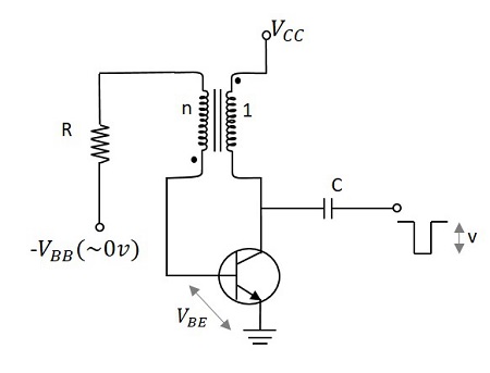
The voltage at the collector is VCC, since the device is OFF. But when a negative trigger is applied at the collector, the voltage gets reduced. Because of the winding polarities of the transformer, the collector voltage goes down, while the base voltage rises.
When the base to emitter voltage becomes greater than the cut-in voltage, i.e.
$$V_{BE} > V_\gamma$$
Then, a small base current is observed. This raises the collector current which decreases the collector voltage. This action cumulates further, which increases the collector current and decreases the collector voltage further. With the regenerative feedback action, if the loop gain increases, the transistor gets into saturation quickly. But this is not a stable state.
Then, a small base current is observed. This raises the collector current which decreases the collector voltage. This action cumulates further, which increases the collector current and decreases the collector voltage further. With the regenerative feedback action, if the loop gain increases, the transistor gets into saturation quickly. But this is not a stable state.
When the transistor gets into saturation, the collector current increases and the base current is constant. Now, the collector current slowly starts charging the capacitor and the voltage at the transformer reduces. Due to the transformer winding polarities, the base voltage gets increased. This in turn decreases the base current. This cumulative action, throws the transistor into cut off condition, which is the stable state of the circuit.
The output waveforms are as follows −
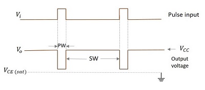
The main disadvantage of this circuit is that the output Pulse width cannot be maintained stable. We know that the collector current is
$$i_c = h_{FE}i_B$$
As the hFE is temperature dependent and the pulse width varies linearly with this, the output pulse width cannot be stable. Also hFE varies with the transistor used.
Anyways, this disadvantage can be eliminated if the resistor is placed in emitter, which means the solution is the emitter timing circuit. When the above condition occurs, the transistor turns OFF in the emitter timing circuit and so a stable output is obtained.
Astable Blocking Oscillator
If the blocking oscillator can change its state automatically, it is called as an Astable blocking oscillator circuit. These Astable blocking oscillators can be of two types. They are
- Diode controlled Astable blocking oscillator
- RC controlled Astable blocking oscillator
In diode controlled Astable blocking oscillator, a diode placed in the collector changes the state of the blocking oscillator. While in the RC controlled Astable blocking oscillator, a timing resistor R and capacitor C form a network in the emitter section to control the pulse timings.
To have a clear understanding, let us discuss the working of Diode controlled Astable blocking oscillator.
Diode controlled Astable blocking oscillator
The diode controlled Astable blocking oscillator contains a pulse transformer in the collector circuit. A capacitor is connected in between transformer secondary and the base of the transistor. The transformer primary and the diode are connected in the collector.
An initial pulse is given at the collector of the transistor to initiate the process and from there no pulses are required and the circuit behaves as an Astable Multivibrator. The figure below shows the circuit of a diode controlled Astable blocking oscillator.
Initially the transistor is in OFF state. To initiate the circuit, a negative trigger pulse is applied at the collector. The diode whose anode is connected to the collector, will be in reverse biased condition and will be OFF by the application of this negative trigger pulse.
This pulse is applied to the pulse transformer and due to the winding polarities (as indicated in the figure), same amount of voltage gets induced without any phase inversion. This voltage flows through the capacitor towards the base, contributing some base current. This base current, develops some base to emitter voltage, which when crosses the cut-in voltage, pushes the transistor Q1 to ON. Now, the collector current of the transistor Q1 raises and it gets applied to both the diode and the transformer. The diode which is initially OFF gets ON now. The voltage that gets induced into the transformer primary windings induces some voltage into the transformer secondary winding, using which the capacitor starts charging.
As the capacitor will not deliver any current while it is getting charged, the base current iB stops flowing. This turns the transistor Q1 OFF. Hence the state is changed.
Now, the diode which was ON, has some voltage across it, which gets applied to the transformer primary, which is induced into the secondary. Now, the current flows through the capacitor which lets the capacitor discharge. Hence the base current iB flows turning the transistor ON again. The output waveforms are as shown below.
As the diode helps the transistor to change its state, this circuit is diode controlled. Also, as the trigger pulse is applied only at the time of initiation, whereas the circuit keeps on changing its state all by its own, this circuit is an Astable oscillator. Hence the name diode controlled Astable blocking oscillator is given.
Another type of circuit uses R and C combination in the emitter portion of the transistor and it is called as RC controlled Astable blocking oscillator circuit.
Pulse Circuits - Sampling Gates
Up to now, we have come across different Pulse circuits. At times, we get the need to restrict the application of such pulse inputs to certain time periods. The circuit that helps us in this aspect is the Sampling gate circuit. These are also called as linear gates or transmission gates or selection circuits.
These sampling gates help in selecting the transmission signal in a certain time interval, for which the output signal is same as input signal or zero otherwise. That time period is selected using a control signal or selection signal.
Sampling Gates
For a Sampling gate, the output signal must be same as the input or proportional to the input signal in a selected time interval and should be zero otherwise. That selected time period is called as Transmission Period and the other time period is called as Non-transmission Period. This is selected using a control signal indicated by VC. The following figure explain this point.
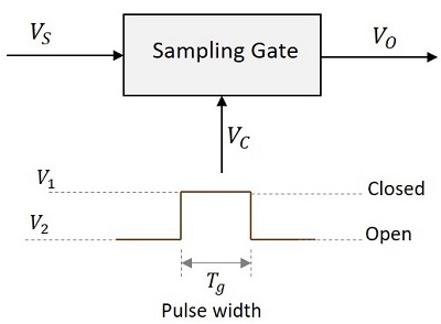
When the control signal VC is at V1, the sampling gate is closed and when VC is at V2, it is open. The pulse width Tg indicates the time period for which the gate pulse is applied.
Types of Sampling Gates
The types of Sampling gates include −
Unidirectional sampling sgates − These type of sampling gates can pass either positive or negative going pulses through them. They are constructed using diodes.
Bidirectional sampling gate − These type of sampling gates can pass both positive and negative going pulses through them. They are constructed using either diodes or BJTs.
Types of Switches Used
The sampling gates can be constructed using series or shunt switches. The time period for which the switch has to be open or close is determined by the gating pulse signal. These switches are replaced by active elements like diodes and transistors.
The following figure shows the block diagrams of sampling gates using series and shunt switches.
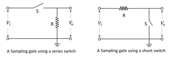
Sampling Gate using a Series Switch
In this type of switch, if the switch S is closed, the output will be exactly equal or proportional to the input. That time period will be the Transmission Period.
If the switch S is open, the output will be zero or ground signal. That time period will be the Non-transmission Period.
Sampling Gate using a Shunt Switch
In this type of switch, if the switch S is closed, the output will be zero or ground signal. That time period will be the Non-transmission Period.
If the switch S is open, the output will be exactly equal or proportional to the input. That time period will be the Transmission Period.
The sampling gates are entirely different from logic gates of digital circuits. They are also represented by pulses or voltage levels. But they are digital gates and their output is not the exact replica of the input. Whereas the sampling gate circuits are the analog gates whose output is exact replica of the input.
In the coming chapters, we will discuss the types of sampling gates.
Unidirectional Sampling Gate
After going through the concept of sampling gates, let us now try to understand the types of sampling gates. Unidirectional sampling gates can pass either positive or negative going pulses through them. They are constructed using diodes.
A unidirectional sampling gate circuit consists of a capacitor C, a diode D and two resistors R1 and RL. The signal input is given to the capacitor and the control input is given to the resistor R1. The output is taken across the load resistor RL. The circuit is as shown below.
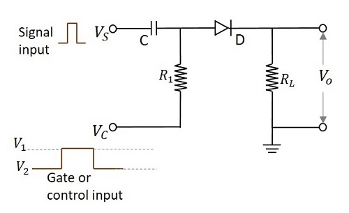
According to the functioning of a diode, it conducts only when the anode of the diode is more positive than the cathode of the diode. If the diode has positive signal at its input, it conducts. The time period in which the gate signal is ON, is the transmission period. Hence it is during that period in which the input signal is transmitted. Otherwise the transmission is not possible.
The following figure shows the time periods of the input signal and the gate signal.
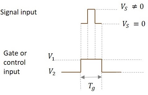
The input signal is transmitted only for the time period during which gate is ON as shown in the figure.
From the circuit we have,
The anode of the diode is applied with the two signals (VS and VC). If the voltage at the anode is indicated as VP and the voltage at the cathode is indicated as VN then the output voltage is obtained as
$$V_o = V_P = (V_S + V_C) > V_N$$
So the diode is in forward biased condition.
$$V_O = V_S + V_1 > V_N$$
Then
$$V_O = V_S$$
When V1 = 0,
Then
$$V_O = V_S + V_1 \: Which \: means \: V_O = V_S$$
Ideal value of V1 = 0.
So, if V1 = 0, the entire input signal appears at output. If the value of V1 is negative, then some of the input is lost and if V1 is positive, additional signal along with input appears at the output.
This whole thing happens during transmission period.
During non-transmission period,
$$V_O = 0$$
As diode is in reverse biased condition
When voltage on anode is less than voltage on cathode,
$$V_S + V_C < 0 \: Volts$$
During non-transmission period,
$$V_C = V_2$$
$$V_S + V_2 < 0$$
Magnitude of V2 should be very high than Vs.
$$|V_2| ≫ V_S$$
Because for the diode to be in reverse bias, the sum of the voltages VS and VC should be negative. VC (which is V2 now) should be as negative as possible so that though VS is positive, the sum of both the voltages should yield a negative result.
Special Cases
Now, lets see a few cases for different values of input voltages where the control voltage is of some negative value.
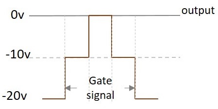
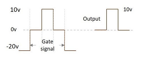
Case 1
Let us take an example where VS = 10V and VC = -10v (V1) to -20v (V2)
Now, when these two signals are applied, (VS and VC) then the voltage at anode will be
$$V_P = V_S + V_C$$
As this is about transmission period, only V1 is considered for VC.
$$V_O = (10V) + (-10V) = 0V$$
Hence the output will be a zero, though some amount of input voltage is being applied. The following figure explains this point.
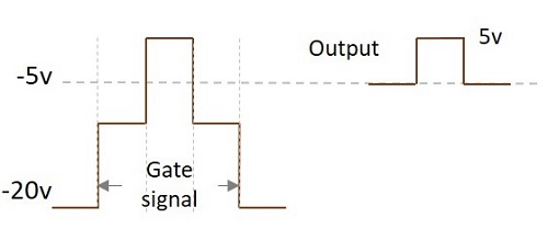
Case 2
Let us take an example where VS = 10V and VC = -5v (V1) to -20v (V2)
Now, when these two signals are applied, (VS and VC) then the voltage at anode will be
$$V_P = V_S + V_C$$
As this is about transmission period, only V1 is considered for VC.
$$V_O = (10V) + (-5V) = 5V$$
Hence the output will be 5 V. The following figure explains this point.
Case 3
Let us take an example where VS = 10V and VC = 0v (V1) to -20v (V2)
Now, when these two signals are applied, (VS and VC) then the voltage at anode will be
$$V_P = V_S + V_C$$
As this is about transmission period, only V1 is considered for VC.
$$V_O = (10V) + (0V) = 10V$$
Hence the output will be a 10 V. The following figure explains this point.
Case 4
Let us take an example where VS = 10V and VC = 5v (V1) to -20v (V2)
Now, when these two signals are applied, (VS and VC) then the voltage at anode will be
$$V_P = V_S + V_C$$
As this is about transmission period, only V1 is considered for VC.
$$V_O = (10V) + (5V) = 15V$$
Hence the output will be a 15 V.
The output voltage gets affected by the control voltage applied. This voltage adds up to the input to produce the output. Hence it affects the output.
The following figure shows the superimposition of both the signals.
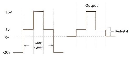
We can observe that during the time when only gate voltage is applied, the output will be 5v. When both the signals are applied, VP appears as VO. During the non-transmission period, output is 0v.
As it is observed from the above figure, the difference in the output signals during transmission period and non-transmission period, though (with VS = 0) input signal is not applied, is called as Pedestal. This pedestal can be positive or negative. In this example, we get a positive pedestal in the output.
Effect of RC on Control voltage
If the input signal is applied before the control voltage reaches the steady state, there occurs some distortion in the output.
We get the correct output only when the input signal is given when control signal is 0v. This 0v is the stable value. If the input signal is given before that, distortion occurs.
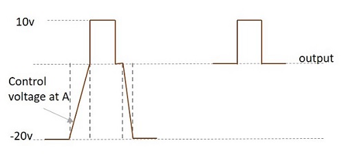
The slow rise in the control voltage at A is due to the RC circuit present. The time constant which is the result of RC affects the shape of this waveform.
Pros and Cons of Unidirectional Sampling Gates
Let us have a look at the advantages and disadvantages of unidirectional sampling gate.
Advantages
The circuitry is simple.
Time delay between input and output is too low.
It can be extended to more number of inputs.
No current is drawn during non-transmission period. Hence under quiescent condition, no power dissipation is present.
Disadvantages
Theres interaction between control and input signals (VC and VS)
As the number of inputs increase, the loading on control input increases.
Output is sensitive to control input voltage V1 (upper level of VC)
Only one input should be applied at one instant of time.
Because of slow rise time of the control signal, the output may get distorted, if the input signal is applied before reaching the steady state.
Unidirectional with More Inputs
The unidirectional sampling gate circuits that we have discussed so far have a single input. In this chapter, let us discuss a few more unidirectional sampling gate circuits that can handle more than one input signals.
A unidirectional sampling gate circuit consists of the capacitors and resistors of same value. Here two input unidirectional diode sampling gate with two inputs is considered. In this circuit we have two capacitors and two resistors of same value. They are connected with two diodes each.
The control signal is applied at the resistors. The output is taken across the load resistor. The figure below shows the circuit diagram for unidirectional diode sampling gate with more than one input signal.
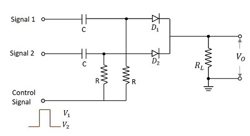
When the control input is given,
At VC = V1 which is during the transmission period, both the diodes D1 and D2 are forward biased. Now, the output will be the sum of all the three inputs.
$$V_O = V_{S1} + V_{S2} + V_C$$
For V1 = 0v which is the ideal value,
$$V_O = V_{S1} + V_{S2}$$
Here we have a major limitation that at any instant of time, during the transmission period, only one input should be applied. This is a disadvantage of this circuit.
During the non-transmission period,
$$V_C = V_2$$
Both the diodes will be in reverse bias which means open circuited.
This makes the output
$$V_O = 0V$$
The main disadvantage of this circuit is that the loading of the circuit increases as the number of inputs increase. This limitation can be avoided by another circuit in which the control input is given after the input signal diodes.
Pedestal Reduction
While going through different types of sampling gates and the outputs they produce, we have come across an extra voltage level in the output waveforms called as Pedestal. This is unwanted and creates some noise.
Reduction of Pedestal in a Gate circuit
The difference in the output signals during transmission period and non-transmission period though the input signals is not applied, is called as Pedestal. It can be a positive or a negative pedestal.
Hence it is the output observed because of the gating voltage though the input signal is absent. This is unwanted and has to be reduced. The circuit below is designed for the reduction of pedestal in a gate circuit.
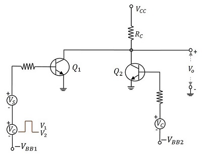
When the control signal is applied, during the transmission period i.e. at V1, Q1 turns ON and Q2 turns OFF and the VCC is applied through RC to Q1. Whereas during the nontransmission period i.e. at V2, Q2 turns ON and Q1 turns OFF and the VCC is applied through RC to Q2. The base voltages VBB1 and VBB2 and the amplitude of gate signals are adjusted so that two transistor currents are identical and as a result the quiescent output voltage level will remain constant.
If the gate pulse voltage is large compared with the VBE of the transistors, then each transistor is biased far below cut off, when it is not conducting. So, when the gate voltage appears, Q2 will be driven into cut off before Q1 starts to conduct, whereas at the end of the gate, Q1 will be driven to cut off before Q2 starts to conduct.
The figure below explains this in a better fashion.
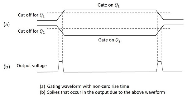
Hence the gate signals appear as in the above figure. The gated signal voltage will appear superimposed on this waveform. These spikes will be of negligible value if the gate waveform rise time is small compared with the gate duration.
There are few drawbacks of this circuit such as
Definite rise and fall times, result in sharp spikes
The continuous current through RC dissipates lot of heat
Two bias voltages and two control signal sources (complement to each other) make the circuit complicated.
Other than these drawbacks, this circuit is useful in the reduction of pedestal in a gate circuit.
Bidirectional Sampling Gates
Bidirectional gates, unlike unidirectional ones, transmit signals of both positive and negative polarities. These gates can be constructed using either transistors or diodes. From different types of circuits, let us go through a circuit made up of transistors and another made up of diodes.
Bidirectional Sampling Gates using Transistors
A basic bidirectional sampling gate consists of a transistor and three resistors. The input signal voltage VS and the control input voltage VC are applied through the summing resistors to the base of the transistor. The circuit diagram given below shows the bidirectional sampling gate using transistor.
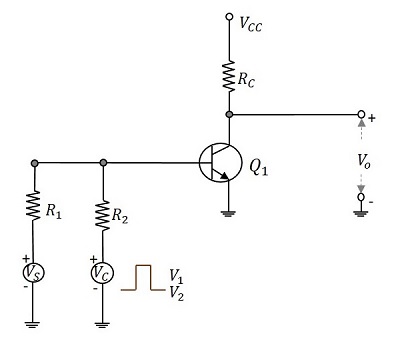
The control input VC applied here is a pulse waveform with two levels V1 and V2 and pulse width tp. This pulse width decides the desired transmission interval. The gating signal allows the input to get transmitted. When the gating signal is at its lower level V2, the transistor goes into active region. So, until the gating input is maintained at its upper level, signals of either polarity, which appear at the base of the transistor will be sampled and appear amplified at the output.
Four Diode Bidirectional Sampling Gate
Bidirectional sampling gate circuit is made using diodes also. A two diode bidirectional sampling gate is the basic one in this model. But it has few disadvantages such as
- It has low gain
- It is sensitive to the imbalances of control voltage
- Vn (min) may be excessive
- Diode capacitance leakage is present
A four diode bidirectional sampling gate was developed, improving these features. A two bidirectional sampling gate circuit was improved adding two more diodes and two balanced voltages +v or v to make the circuit of a four diode bidirectional sampling gate as shown in the figure.
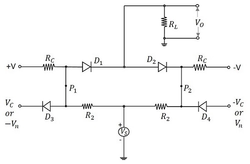
The control voltages VC and VC reverse bias the diodes D3 and D4 respectively. The voltages +v and v forward bias the diodes D1 and D2 respectively. The signal source is coupled to the load through the resistors R2 and the conducting diodes D1 and D2. As the diodes D3 and D4 are reverse biased, they are open and disconnect the control signals from gate. So, an imbalance in control signals will not affect the output.
When the control voltages applied are Vn and Vn, then the diodes D3 and D4 conduct. The points P2 and P1 are clamped to these voltages, which make the diodes D1 and D2 revere biased. Now, the output is zero.
During transmission, the diodes D3 and D4 are OFF. The gain A of the circuit is given by
$$A = \frac{R_C}{R_C + R_2} \times \frac{R_L}{R_L + (R_s/2)}$$
Hence the choice of application of control voltages enables or disables the transmission. The signals of either polarities are transmitted depending upon the gating inputs.
Applications of Sampling Gates
There are many applications of sampling gate circuits. The most common ones are as follows −
- Sampling scopes
- Multiplexers
- Sample and hold circuits
- Digital to Analog Converters
- Chopped Stabilizer Amplifiers
Among the applications of sampling gate circuits, the Sampling scope circuit is prevalent. Let us try to have an idea on the block diagram of sampling scope.
Sampling Scope
In the sampling scope, the display consists of a sequence of samples of input waveform. Each of those samples are taken at a time progressively delayed with respect to some reference point in the waveform. This is the working principle of sampling scope which is shown below in the block diagram.
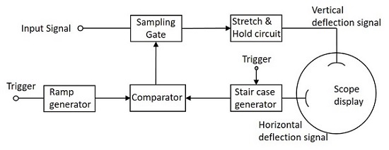
The ramp generator and the stair case generator generates the waveforms according to the trigger inputs applied. The comparator compares both of these signals and generates the output which is then given to the sampling gate circuit as a control signal.
As and when the control input is high the input at the sampling gate is delivered to the output and whenever the control input is low, the input is not transmitted.
While taking the samples, they are chosen at the time instants, which are progressively delayed by equal increments. The samples consist of a pulse whose duration is equal to the duration of the sampling gate control and whose amplitude is determined by the magnitude of the input signal at the sampling time. The pulse width then produced will be low.
Just like in the Pulse modulation, the signal has to be sampled and hold. But as the pulse width is low, it is amplified by an amplifier circuit so as to stretch and then given to a diode-capacitor combination circuit so as to hold the signal, to fill the interval of the next sample. The output this circuit is given to the vertical deflection plates and the output of sweep circuit is given to the horizontal deflection plates of the sampling scope to display the output waveform.
