- Pulse Circuits Time Base Generators
- Time Base Generators (Overview)
- Types of Time Base Generators
- Bootstrap Time Base Generator
- Miller Sweep Generator
- Pulse Circuits Sweep Circuits
- Unijunction Transistor
- UJT as Relaxation Oscillator
- Pulse Circuits - Synchronization
- Pulse Circuits - Blocking Oscillators
- Pulse Circuits Sampling Gates
- Pulse Circuits - Sampling Gates
- Unidirectional Sampling Gate
- Unidirectional with More Inputs
- Bidirectional Sampling Gates
- Pulse Circuits Useful Resources
- Pulse Circuits - Quick Guide
- Pulse Circuits - Useful Resources
- Pulse Circuits - Discussion
Unidirectional with More Inputs
The unidirectional sampling gate circuits that we have discussed so far have a single input. In this chapter, let us discuss a few more unidirectional sampling gate circuits that can handle more than one input signals.
A unidirectional sampling gate circuit consists of the capacitors and resistors of same value. Here two input unidirectional diode sampling gate with two inputs is considered. In this circuit we have two capacitors and two resistors of same value. They are connected with two diodes each.
The control signal is applied at the resistors. The output is taken across the load resistor. The figure below shows the circuit diagram for unidirectional diode sampling gate with more than one input signal.
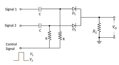
When the control input is given,
At VC = V1 which is during the transmission period, both the diodes D1 and D2 are forward biased. Now, the output will be the sum of all the three inputs.
$$V_O = V_{S1} + V_{S2} + V_C$$
For V1 = 0v which is the ideal value,
$$V_O = V_{S1} + V_{S2}$$
Here we have a major limitation that at any instant of time, during the transmission period, only one input should be applied. This is a disadvantage of this circuit.
During the non-transmission period,
$$V_C = V_2$$
Both the diodes will be in reverse bias which means open circuited.
This makes the output
$$V_O = 0V$$
The main disadvantage of this circuit is that the loading of the circuit increases as the number of inputs increase. This limitation can be avoided by another circuit in which the control input is given after the input signal diodes.
Pedestal Reduction
While going through different types of sampling gates and the outputs they produce, we have come across an extra voltage level in the output waveforms called as Pedestal. This is unwanted and creates some noise.
Reduction of Pedestal in a Gate circuit
The difference in the output signals during transmission period and non-transmission period though the input signals is not applied, is called as Pedestal. It can be a positive or a negative pedestal.
Hence it is the output observed because of the gating voltage though the input signal is absent. This is unwanted and has to be reduced. The circuit below is designed for the reduction of pedestal in a gate circuit.
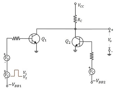
When the control signal is applied, during the transmission period i.e. at V1, Q1 turns ON and Q2 turns OFF and the VCC is applied through RC to Q1. Whereas during the nontransmission period i.e. at V2, Q2 turns ON and Q1 turns OFF and the VCC is applied through RC to Q2. The base voltages VBB1 and VBB2 and the amplitude of gate signals are adjusted so that two transistor currents are identical and as a result the quiescent output voltage level will remain constant.
If the gate pulse voltage is large compared with the VBE of the transistors, then each transistor is biased far below cut off, when it is not conducting. So, when the gate voltage appears, Q2 will be driven into cut off before Q1 starts to conduct, whereas at the end of the gate, Q1 will be driven to cut off before Q2 starts to conduct.
The figure below explains this in a better fashion.
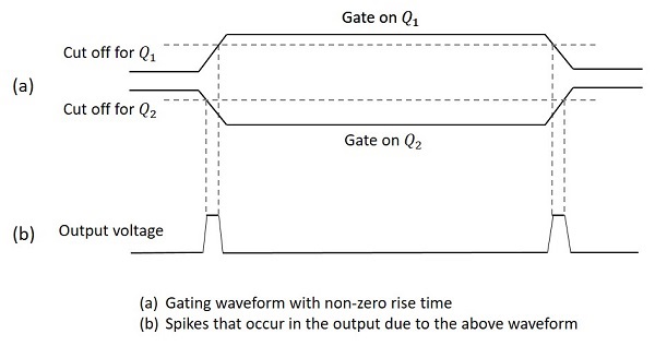
Hence the gate signals appear as in the above figure. The gated signal voltage will appear superimposed on this waveform. These spikes will be of negligible value if the gate waveform rise time is small compared with the gate duration.
There are few drawbacks of this circuit such as
Definite rise and fall times, result in sharp spikes
The continuous current through RC dissipates lot of heat
Two bias voltages and two control signal sources (complement to each other) make the circuit complicated.
Other than these drawbacks, this circuit is useful in the reduction of pedestal in a gate circuit.
