- Pulse Circuits Time Base Generators
- Time Base Generators (Overview)
- Types of Time Base Generators
- Bootstrap Time Base Generator
- Miller Sweep Generator
- Pulse Circuits Sweep Circuits
- Unijunction Transistor
- UJT as Relaxation Oscillator
- Pulse Circuits - Synchronization
- Pulse Circuits - Blocking Oscillators
- Pulse Circuits Sampling Gates
- Pulse Circuits - Sampling Gates
- Unidirectional Sampling Gate
- Unidirectional with More Inputs
- Bidirectional Sampling Gates
- Pulse Circuits Useful Resources
- Pulse Circuits - Quick Guide
- Pulse Circuits - Useful Resources
- Pulse Circuits - Discussion
Pulse Circuits - Blocking Oscillators
An oscillator is a circuit that provides an alternating voltage or current by its own, without any input applied. An Oscillator needs an amplifier and also a feedback from the output. The feedback provided should be regenerative feedback which along with the portion of the output signal, contains a component in the output signal, which is in phase with the input signal. An oscillator that uses a regenerative feedback to generate a nonsinusoidal output is called as Relaxation Oscillator.
We have already seen UJT relaxation oscillator. Another type of relaxation oscillator is the Blocking oscillator.
Blocking Oscillator
A blocking oscillator is a waveform generator that is used to produce narrow pulses or trigger pulses. While having the feedback from the output signal, it blocks the feedback, after a cycle, for certain predetermined time. This feature of blocking the output while being an oscillator, gets the name blocking oscillator to it.
In the construction of a blocking oscillator, the transistor is used as an amplifier and the transformer is used for feedback. The transformer used here is a Pulse transformer. The symbol of a pulse transformer is as shown below.
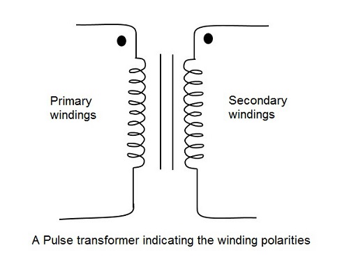
Pulse Transformer
A Pulse transformer is one which couples a source of rectangular pulses of electrical energy to the load. Keeping the shape and other properties of pulses unchanged. They are wide band transformers with minimum attenuation and zero or minimum phase change.
The output of the transformer depends upon the charge and discharge of the capacitor connected.
The regenerative feedback is made easy by using pulse transformer. The output can be fed back to the input in the same phase by properly choosing the winding polarities of the pulse transformer. Blocking oscillator is such a free-running oscillator made using a capacitor and a pulse transformer along with a single transistor which is cut off for most of the duty cycle producing periodic pulses.
Using the blocking oscillator, Astable and Monostable operations are possible. But Bistable operation is not possible. Let us go through them.
Monostable Blocking Oscillator
If the blocking oscillator needs a single pulse, to change its state, it is called as a Monostable blocking oscillator circuit. These Monostable blocking oscillators can be of two types. They are
- Monostable blocking oscillator with base timing
- Monostable blocking oscillator with emitter timing
In both of these, a timing resistor R controls the gate width, which when placed in the base of transistor becomes base timing circuit and when placed in the emitter of transistor becomes emitter timing circuit.
To have a clear understanding, let us discuss the working of base timing Monostable Multivibrator.
Transistor Triggered Monostable blocking oscillator with Base timing
A transistor, a pulse transformer for feedback and a resistor in the base of the transistor constitute the circuit of a transistor triggered Monostable blocking oscillator with base timing. The pulse transformer used here has a turns ratio of n: 1 where the base circuit has n turns for every turn on the collector circuit. A resistance R is connected in series to the base of the transistor which controls the pulse duration.
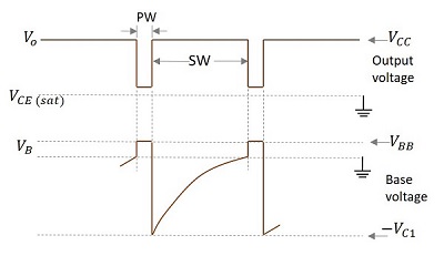
Initially the transistor is in OFF condition. As shown in the following figure, VBB is considered zero or too low, which is negligible.
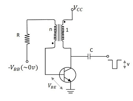
The voltage at the collector is VCC, since the device is OFF. But when a negative trigger is applied at the collector, the voltage gets reduced. Because of the winding polarities of the transformer, the collector voltage goes down, while the base voltage rises.
When the base to emitter voltage becomes greater than the cut-in voltage, i.e.
$$V_{BE} > V_\gamma$$
Then, a small base current is observed. This raises the collector current which decreases the collector voltage. This action cumulates further, which increases the collector current and decreases the collector voltage further. With the regenerative feedback action, if the loop gain increases, the transistor gets into saturation quickly. But this is not a stable state.
Then, a small base current is observed. This raises the collector current which decreases the collector voltage. This action cumulates further, which increases the collector current and decreases the collector voltage further. With the regenerative feedback action, if the loop gain increases, the transistor gets into saturation quickly. But this is not a stable state.
When the transistor gets into saturation, the collector current increases and the base current is constant. Now, the collector current slowly starts charging the capacitor and the voltage at the transformer reduces. Due to the transformer winding polarities, the base voltage gets increased. This in turn decreases the base current. This cumulative action, throws the transistor into cut off condition, which is the stable state of the circuit.
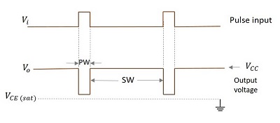
The output waveforms are as follows −
The main disadvantage of this circuit is that the output Pulse width cannot be maintained stable. We know that the collector current is
$$i_c = h_{FE}i_B$$
As the hFE is temperature dependent and the pulse width varies linearly with this, the output pulse width cannot be stable. Also hFE varies with the transistor used.
Anyways, this disadvantage can be eliminated if the resistor is placed in emitter, which means the solution is the emitter timing circuit. When the above condition occurs, the transistor turns OFF in the emitter timing circuit and so a stable output is obtained.
Astable Blocking Oscillator
If the blocking oscillator can change its state automatically, it is called as an Astable blocking oscillator circuit. These Astable blocking oscillators can be of two types. They are
- Diode controlled Astable blocking oscillator
- RC controlled Astable blocking oscillator
In diode controlled Astable blocking oscillator, a diode placed in the collector changes the state of the blocking oscillator. While in the RC controlled Astable blocking oscillator, a timing resistor R and capacitor C form a network in the emitter section to control the pulse timings.
To have a clear understanding, let us discuss the working of Diode controlled Astable blocking oscillator.
Diode controlled Astable blocking oscillator
The diode controlled Astable blocking oscillator contains a pulse transformer in the collector circuit. A capacitor is connected in between transformer secondary and the base of the transistor. The transformer primary and the diode are connected in the collector.
An initial pulse is given at the collector of the transistor to initiate the process and from there no pulses are required and the circuit behaves as an Astable Multivibrator. The figure below shows the circuit of a diode controlled Astable blocking oscillator.
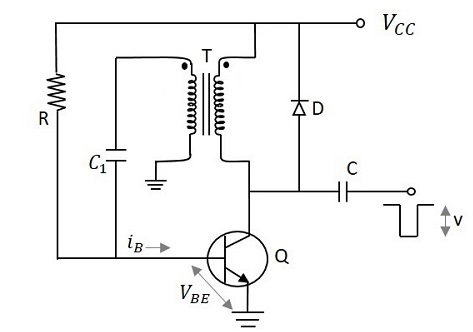
Initially the transistor is in OFF state. To initiate the circuit, a negative trigger pulse is applied at the collector. The diode whose anode is connected to the collector, will be in reverse biased condition and will be OFF by the application of this negative trigger pulse.
This pulse is applied to the pulse transformer and due to the winding polarities (as indicated in the figure), same amount of voltage gets induced without any phase inversion. This voltage flows through the capacitor towards the base, contributing some base current. This base current, develops some base to emitter voltage, which when crosses the cut-in voltage, pushes the transistor Q1 to ON. Now, the collector current of the transistor Q1 raises and it gets applied to both the diode and the transformer. The diode which is initially OFF gets ON now. The voltage that gets induced into the transformer primary windings induces some voltage into the transformer secondary winding, using which the capacitor starts charging.
As the capacitor will not deliver any current while it is getting charged, the base current iB stops flowing. This turns the transistor Q1 OFF. Hence the state is changed.
Now, the diode which was ON, has some voltage across it, which gets applied to the transformer primary, which is induced into the secondary. Now, the current flows through the capacitor which lets the capacitor discharge. Hence the base current iB flows turning the transistor ON again. The output waveforms are as shown below.
As the diode helps the transistor to change its state, this circuit is diode controlled. Also, as the trigger pulse is applied only at the time of initiation, whereas the circuit keeps on changing its state all by its own, this circuit is an Astable oscillator. Hence the name diode controlled Astable blocking oscillator is given.
Another type of circuit uses R and C combination in the emitter portion of the transistor and it is called as RC controlled Astable blocking oscillator circuit.