
Article Categories
- All Categories
-
 Data Structure
-
 Networking
-
 RDBMS
RDBMS
-
 Operating System
-
 Java
Java
-
 MS Excel
-
 iOS
iOS
-
 HTML
HTML
-
 CSS
CSS
-
 Android
-
 Python
-
 C Programming
-
 C++
C++
-
 C#
C#
-
 MongoDB
-
 MySQL
MySQL
-
 Javascript
-
 PHP
PHP
-
 Economics & Finance
Pin diagram of 8212
We find 8212 available in nowadays as a package chip which is dual inline having 24 pins total. We find its functional pin diagram below.
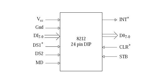
Fig: Pin diagram of 8212 functional
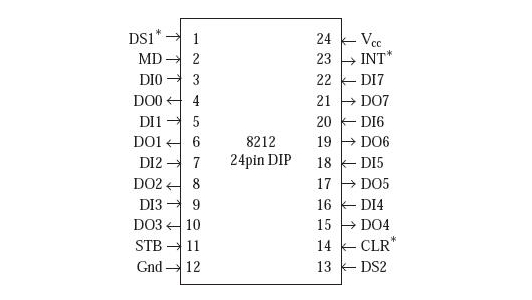
Fig: Pin diagram of 8212
Voltage of + 5 V is required for it to work based on the supply which is DC. The latch which is 8 bit in 8212 receives the information which is present on the eight data inputs ranging from DI7 to D10. The condition which helps in information latching is present on DI7 to DI0 depends on the state of logic of the pin which is of mode MD. The information which is present in the latch comes out on the data output pins ranging from D7-D0. The condition which is satisfied for the information to be latched comes out is dependent MD pin.
We have D-type flip-flop which is edge-triggered depends on 8212. We call it the service request flip-flop. It is responsible for generating an interrupt request on the pin INT*. INT* is an active low output pin, which is useful in interrupt-driven data transfer scheme. The internal architecture which is responsible for activating the INT* signal is shown below
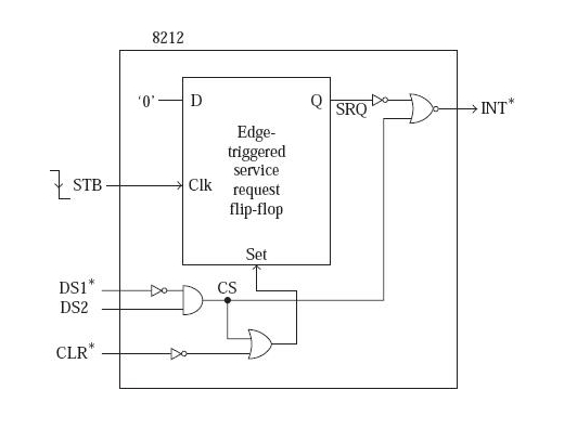
Fig: Circuit responsible for activating INT* in 8212
We can see from the above fig that INT* gets activated in the two cases stated below.
The internal chip select signal gets activated when DS1* is 0 and DS2 is 1.
When a high to low transition is done by STB so that the internal signal which is SQ is 0.
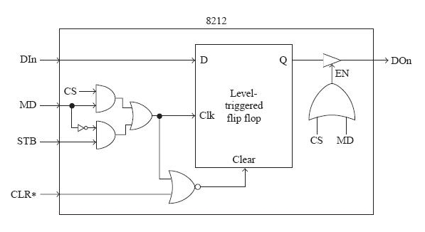
Fig: Connection details for a flip flop latch in 8212
The following conclusions which are drawn from the fig shows that. When MD is equal to 1, CS acts latches for clock. When MD is equal to 0, STB acts as the clock for the latches. When the clock is in high state, the output Q of the latch follows input corresponding DI. When the high to low transition is made by the clock, latching of the data gets into action. The data at the output Q gets out on the pin corresponding DO when the EN signal gets activated. The EN signal gets activated whenever CS is equal to 1 or MD is equal to 1.
In brief lets gets the outline of the pins −
| Vcc: |
Always gets connected to the dc corresponding to +5V |
| Gnd |
Gets connected to ground |
| MD |
It is the Mode input pin. determines the clock sources to latches. If MD is 0, STB acts as the clock input to the latches. If where as if MD is 1, CS acts as the input of the clock. |
| STB |
It is Strobe input. |
| DS1*, DS2 |
These are the devices which select pins. |
| DI7-0 |
These are the eight Data inputs ranging from D7 to D0. |
| DO7-0 |
Data outputs. |
| INT* |
It is the Interrupt output pin which is Used for interrupting the microprocessor. |
| CLR* |
It is an asynchronous clear input which is actively low. |

688 Views
