
Article Categories
- All Categories
-
 Data Structure
-
 Networking
-
 RDBMS
RDBMS
-
 Operating System
-
 Java
Java
-
 MS Excel
-
 iOS
iOS
-
 HTML
HTML
-
 CSS
CSS
-
 Android
-
 Python
-
 C Programming
-
 C++
C++
-
 C#
C#
-
 MongoDB
-
 MySQL
MySQL
-
 Javascript
-
 PHP
PHP
-
 Economics & Finance
Intel 8212 in mode 1
The figure below shows the working of 8212 in mode 1
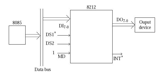
Fig: Working of 8212 in mode 1
We use this mode generally when we want 8212 to function as an output port. Here, microprocessor drives DI7-0, and the device at the output receives the information on Do7-0. The clock to the latches is provided in this mode. 8212 latches the information on DI7-0 when the CS makes transition from high to low. The CS signal gets activates when INT* is transferred by the interrupts by the driven data transfer scheme which is always performed when desired. The buffer at the output gets enabled in this mode. So the latched information which is of 8 bit straightaway comes out on Do7 to Do0 without any given conditions.
Let's discuss the Following two applications
Low order address latch
Output port which is interrupting.
Intel 8212 as low-order address latch: Here the low-order address lines and data lines are multiplexed and are available as AD7-0. It is convenient to have the address as many times and the separation of data on the different lines. Let's for an example, if we connect a chip like 2716 in an 8085-based system, the 2716 needs bit address of11 bits in its address pins, and here is separate 8 pins kept for data. Now connecting the AD7-0 pins of 8085 to the LS 8 address pins of 2716, the address will only be available for the only one clock cycle in a complete machine cycle. Thus, de-multiplexing of address and data is needed
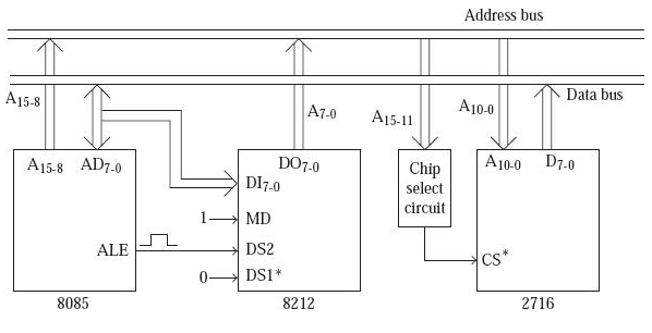
Fig. 8212 low order address latch
Intel 8212 as an interrupting output port: When any output device wants to perform the driven interrupt data transfer, a positive pulse is send on the STB pin.

449 Views
