
Article Categories
- All Categories
-
 Data Structure
-
 Networking
-
 RDBMS
RDBMS
-
 Operating System
-
 Java
Java
-
 MS Excel
-
 iOS
iOS
-
 HTML
HTML
-
 CSS
CSS
-
 Android
-
 Python
-
 C Programming
-
 C++
C++
-
 C#
C#
-
 MongoDB
-
 MySQL
MySQL
-
 Javascript
-
 PHP
PHP
-
 Economics & Finance
Selected Reading
Pin description of 6800
The Motorola M6800 is 40pin DIP Microprocessor. Here we will see the actual pin level diagram of M6800 and also the functional pin diagram of it.
The M6800 requires some additional chips to provide the required functions. These chips are:
6870 (clock generator)
6830 (ROM) or 68708(EPROM)
6810 (RAM)
6820 (PeripheralInterface Adapter)
6850 (AsynchronousCommunications Interface Adapter)
6828 (PriorityInterrupt Controller)
Now see the Pin Level diagram of Motorola M6800
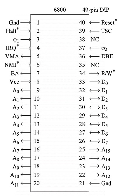
This is the actual pin diagram of the M6800 Microprocessor. Now we will see the functional pin diagram of it.
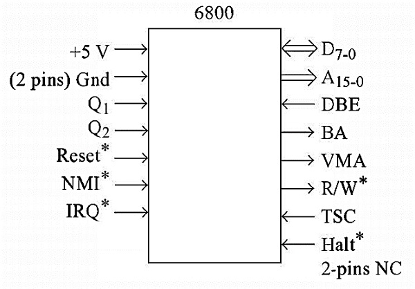
Now let us see the Pin functions of the M6800 microprocessor.
| Pins |
Type |
Function |
|---|---|---|
|
A15– A0 |
Output |
16-bit address bus, which provides the addresses for memory (up to 64KB) |
| D7– D0 |
Input/Output |
8-bit bi-directional data bus to transfer data between memory/IO devices and CPU. |
|
Vcc |
Input |
It is Power Supply Pin of M6800. It uses DC power supply of +5V |
|
GND |
Input |
There are two ground pins (Pin number 1 and 21), both are connected with the ground |
| HALT | Input |
The Halt Pin is active low, input pin. When it is activated, the CPU goes to the halting state. In this state, the address bus, and the data bus, and also R/W the go-to high impedance state. |
|
φ1 and φ2 |
Input |
These are basically two-phase clock inputs. It needs a clock generator chip M6870 to provide a two-phase clock. The typical operating frequency is 1MHz and the minimum frequency is 100KHz. |
|
IRQ |
Input |
This pin is for an Interrupt request. It can be masked or disabled. |
|
TSC |
Input |
It is an active high input pin. It is translated Control pin. This pin is like the hold input of Intel8085 Microprocessor. |
|
BA |
Output |
It is another Active high output pin. BA stands for Bus Available. In 8085, there is HLDA pin, which is similar to the BA pin of M6800. |
|
R/W |
Output |
This is active low output pin. TheCPU sends 1 in this pin, when it tries to read the data, and sends 0, when tries to write data to the memory. |
| NMI | Input |
This is active low Non-Maskable Interrupt pin. |
| RESET | Input |
It is active low input pin. When low signal is passed the M6800 is reset. |
|
VMA |
Output |
VMA is active high output pin. It is valid Memory Access. When the pin is activated, it indicates that the address bus is holding a valid address. It is activated a little after the address is send via address bus. |
|
DBE |
Input |
DBE is active high Input pin. The name suggests Data Bus Enable.So, when this pin is high, either the data are coming out from the data bus or going in through the data bus. But when it islow, it means the data bus pins are in tristate condition.Generally it is connected to pin. |
|
NC |
---- |
The NC are NoConnection. In this clip, there are two NC pins |

Updated on: 2020-06-27T13:36:16+05:30
2K+ Views

Advertisements