
Article Categories
- All Categories
-
 Data Structure
-
 Networking
-
 RDBMS
RDBMS
-
 Operating System
-
 Java
Java
-
 MS Excel
-
 iOS
iOS
-
 HTML
HTML
-
 CSS
CSS
-
 Android
-
 Python
-
 C Programming
-
 C++
C++
-
 C#
C#
-
 MongoDB
-
 MySQL
MySQL
-
 Javascript
-
 PHP
PHP
-
 Economics & Finance
Working of 8212
There are two types of Input Output ports. They are Programmable Input Output ports and Non-Programmable Input Output ports. Since the functions of Programmable Input Output ports changed by software they became more popular. We don't need to change the wiring rather the hardware of the I/O port to change the function. Intel 8255 is a popular Input Output chip based on port. Whereas the I/O ports which are non-programmable needs to change the wiring or the hardware to change its complete function. We will see in later that the connection needs to be changed when 8212 works like an input port in place of output port. These Input Output ports which are non-programmable are designed in a simple way.
We find 8212 available in nowadays as a package chip which is dual inline having 24 pins total. We find its functional pin diagram below.
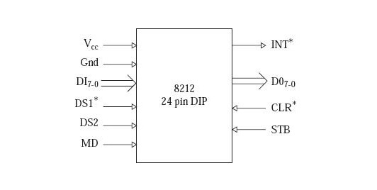
Fig: Pin diagram of 8212 functional
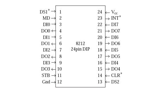
Fig: Pin diagram of 8212
Voltage of + 5 V is required for it to work based on the supply which is DC. The latch which is 8 bit in 8212 receives the information which is present on the eight data inputs ranging from DI7 to D10. The condition which helps in information latching is present on DI7 toDI0 depends on the state of logic of the pin which is of mode MD. The information which is present in the latch comes out on the data output pins ranging from D7-D0. The condition which is satisfied for the information to be latched comes out is dependent MD pin.
We have D-type flip-flop which is edge-triggered depends on 8212. We call it the service request flip-flop. It is responsible for generating an interrupt request on the pin INT*. INT* is an active low output pin, which is useful in interrupt-driven data transfer scheme. The internal architecture which is responsible for activating the INT* signal is shown below
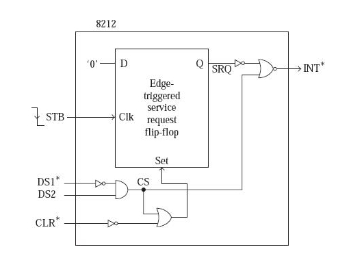
Fig: Circuit responsible for activating INT* in 8212

702 Views
