
- Microprocessor - Home
- Microprocessor Overview
- Microprocessor Classification
- Microprocessor Evolution
- Microprocessor Components
- Microprocessor Characteristics
- Microprocessor Functions
- Microprocessor Pros & Cons
- Microprocessor Application
- Microcontrollers Types
- Microcontrollers Pros & Cons
- 8085 Microprocessor Architecture
- 8085 Microprocessor Pin Configuration
- Addressing Modes & Interrupts
- 8085 Microprocessor Instruction Sets
- 8085 Microprocessor Features
- Externally Initiated Operations
- 8086 Microprocessor
- 8086 Microprocessor Overview
- Functional Units
- Pin Configuration
- Instruction Sets
- 8086 Microprocessor Interrupts
- 8086 Microprocessor Addressing Modes
- 8086 Microprocessor Features
- Memory Segmentation
- Auxiliary Carry Flag
- Maximum and Minimum Mode Configurations
- Multiprocessor Configuration
- Configuration Overview
- 8087 Numeric Data Processor
- I/O Interfacing
- I/O Interfacing Overview
- 8279 Programmable Keyboard
- 8257 DMA Controller
- Serial vs Parallel Communication
- Serial Communications Interface
- Parallel Communication Interface
- 8051 Microcontrollers
- Microcontrollers Overview
- 8051 Microcontrollers Architecture
- 8051 Pin Description
- 8051 Input Output Ports
- 8051 Microcontrollers Interrupts
- Instruction Sets
- Logical Instructions in AVR
- Conditional Branch Instructions AVR
- Arithmetic Instructions in AVR
- External Memory Interfacing
- Time Delay in AVR
- 8051 vs PIC Microcontroller
- Peripheral Devices
- Peripheral Devices
- Programmable Peripheral Interface
- Intel 8255A Pin Description
- Programmable Interval Timer
- 8253/54 Operational Modes
- Interfacing Devices
- Applications and Furture Trends
- Microcontrollers - Application
- Microprocessors and Microcontrollers in IoT
- Microcontrollers in Automotive Systems
- Microcontrollers - Low-Power
- Artificial Intelligence Processors
- Microprocessor Useful Resources
- Microprocessor - Quick Guide
- Microprocessor - Useful Resources
- Microprocessor - Discussion
Microprocessor - 8086 Pin Configuration
8086 was the first 16-bit microprocessor available in 40-pin DIP (Dual Inline Package) chip. Let us now discuss in detail the pin configuration of a 8086 Microprocessor.
8086 Pin Diagram
Here is the pin diagram of 8086 microprocessor −
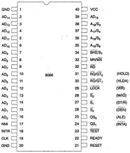
Let us now discuss the signals in detail −
Power supply and frequency signals
It uses 5V DC supply at VCC pin 40, and uses ground at VSS pin 1 and 20 for its operation.
Clock signal
Clock signal is provided through Pin-19. It provides timing to the processor for operations. Its frequency is different for different versions, i.e. 5MHz, 8MHz and 10MHz.
Address/data bus
AD0-AD15. These are 16 address/data bus. AD0-AD7 carries low order byte data and AD8AD15 carries higher order byte data. During the first clock cycle, it carries 16-bit address and after that it carries 16-bit data.
Address/status bus
A16-A19/S3-S6. These are the 4 address/status buses. During the first clock cycle, it carries 4-bit address and later it carries status signals.
S7/BHE
BHE stands for Bus High Enable. It is available at pin 34 and used to indicate the transfer of data using data bus D8-D15. This signal is low during the first clock cycle, thereafter it is active.
Read($\overline{RD}$)
It is available at pin 32 and is used to read signal for Read operation.
Ready
It is available at pin 22. It is an acknowledgement signal from I/O devices that data is transferred. It is an active high signal. When it is high, it indicates that the device is ready to transfer data. When it is low, it indicates wait state.
RESET
It is available at pin 21 and is used to restart the execution. It causes the processor to immediately terminate its present activity. This signal is active high for the first 4 clock cycles to RESET the microprocessor.
INTR
It is available at pin 18. It is an interrupt request signal, which is sampled during the last clock cycle of each instruction to determine if the processor considered this as an interrupt or not.
NMI
It stands for non-maskable interrupt and is available at pin 17. It is an edge triggered input, which causes an interrupt request to the microprocessor.
$\overline{TEST}$
This signal is like wait state and is available at pin 23. When this signal is high, then the processor has to wait for IDLE state, else the execution continues.
MN/$\overline{MX}$
It stands for Minimum/Maximum and is available at pin 33. It indicates what mode the processor is to operate in; when it is high, it works in the minimum mode and vice-aversa.
INTA
It is an interrupt acknowledgement signal and id available at pin 24. When the microprocessor receives this signal, it acknowledges the interrupt.
ALE
It stands for address enable latch and is available at pin 25. A positive pulse is generated each time the processor begins any operation. This signal indicates the availability of a valid address on the address/data lines.
DEN
It stands for Data Enable and is available at pin 26. It is used to enable Transreceiver 8286. The transreceiver is a device used to separate data from the address/data bus.
DT/R
It stands for Data Transmit/Receive signal and is available at pin 27. It decides the direction of data flow through the transreceiver. When it is high, data is transmitted out and vice-a-versa.
M/IO
This signal is used to distinguish between memory and I/O operations. When it is high, it indicates I/O operation and when it is low indicates the memory operation. It is available at pin 28.
WR
It stands for write signal and is available at pin 29. It is used to write the data into the memory or the output device depending on the status of M/IO signal.
HLDA
It stands for Hold Acknowledgement signal and is available at pin 30. This signal acknowledges the HOLD signal.
HOLD
This signal indicates to the processor that external devices are requesting to access the address/data buses. It is available at pin 31.
QS1 and QS0
These are queue status signals and are available at pin 24 and 25. These signals provide the status of instruction queue. Their conditions are shown in the following table −
| QS0 | QS1 | Status |
|---|---|---|
| 0 | 0 | No operation |
| 0 | 1 | First byte of opcode from the queue |
| 1 | 0 | Empty the queue |
| 1 | 1 | Subsequent byte from the queue |
S0, S1, S2
These are the status signals that provide the status of operation, which is used by the Bus Controller 8288 to generate memory & I/O control signals. These are available at pin 26, 27, and 28. Following is the table showing their status −
| S2 | S1 | S0 | Status |
|---|---|---|---|
| 0 | 0 | 0 | Interrupt acknowledgement |
| 0 | 0 | 1 | I/O Read |
| 0 | 1 | 0 | I/O Write |
| 0 | 1 | 1 | Halt |
| 1 | 0 | 0 | Opcode fetch |
| 1 | 0 | 1 | Memory read |
| 1 | 1 | 0 | Memory write |
| 1 | 1 | 1 | Passive |
LOCK
When this signal is active, it indicates to the other processors not to ask the CPU to leave the system bus. It is activated using the LOCK prefix on any instruction and is available at pin 29.
RQ/GT1 and RQ/GT0
These are the Request/Grant signals used by the other processors requesting the CPU to release the system bus. When the signal is received by CPU, then it sends acknowledgment. RQ/GT0 has a higher priority than RQ/GT1.