
Article Categories
- All Categories
-
 Data Structure
-
 Networking
-
 RDBMS
RDBMS
-
 Operating System
-
 Java
Java
-
 MS Excel
-
 iOS
iOS
-
 HTML
HTML
-
 CSS
CSS
-
 Android
-
 Python
-
 C Programming
-
 C++
C++
-
 C#
C#
-
 MongoDB
-
 MySQL
MySQL
-
 Javascript
-
 PHP
PHP
-
 Economics & Finance
Mode 1—strobed I/O
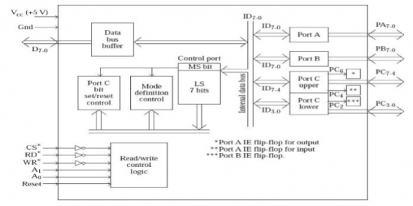
We call mode 1 as the strobed Input Output or handshake Input Output. We use this mode when the data is supplied by the input device to the microprocessor at irregular interval of time. A port which is functioned to program in mode uses three handshake signals. These handshake signals are provided by Port C. Only port A and B works in mode 1. The pins PC2, PC1, and PC0 provides handshake signals for port B when we configure it for Input port or Output port. Moreover, the pins PC7, PC6, and PC3 provides handshake signals for port A. The point to be noted that PC3 pin is a handshake line for Port A in the input terminal and also performing the output operations. If port A and B both works in mode 1 the remaining two pins of port C are used for performing the simple Input Output operations in mode 0. If either of Port A or B works in mode 1 then the rest 5 pins of port C are completely free.
Example 1: Configure Port A as strobed input port, Port B as strobed output port, and PC7, PC6 as output lines.
The required mode definition control word is shown in the figure below −
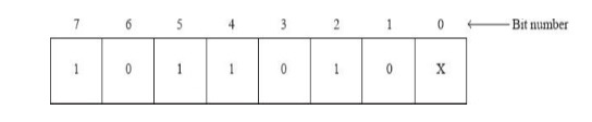
It is to be noted that the LS bit is a don't care bit. This is because all the four lines of Port C
lower are used for handshaking purposes some of which will be input pins and some others outputs. The 8255 will automatically configure these handshake pins, and so it is unimportant whether this LS bit is a 0 or a 1.
Bit 3 must be a 0 to indicate that PC7 and PC6 are output lines. In this case it does not mean that
the entire Port C upper is output, as PC5 and PC4 are used for handshaking purposes. The instructions to achieve this requirement assuming the chip select circuit are as follows.
MVI A, B4H ; Treating X as 0
OUT 23H

2K+ Views
