- Microprocessor - Home
- Microprocessor Overview
- Microprocessor Classification
- Microprocessor Evolution
- Microprocessor Components
- Microprocessor Characteristics
- Microprocessor Functions
- Microprocessor Pros & Cons
- Microprocessor Application
- Microcontrollers Types
- Microcontrollers Pros & Cons
- 8085 Microprocessor Architecture
- 8085 Microprocessor Pin Configuration
- Addressing Modes & Interrupts
- 8085 Microprocessor Instruction Sets
- 8085 Microprocessor Features
- Externally Initiated Operations
- 8086 Microprocessor
- 8086 Microprocessor Overview
- Functional Units
- Pin Configuration
- Instruction Sets
- 8086 Microprocessor Interrupts
- 8086 Microprocessor Addressing Modes
- 8086 Microprocessor Features
- Memory Segmentation
- Auxiliary Carry Flag
- Maximum and Minimum Mode Configurations
- Multiprocessor Configuration
- Configuration Overview
- 8087 Numeric Data Processor
- I/O Interfacing
- I/O Interfacing Overview
- 8279 Programmable Keyboard
- 8257 DMA Controller
- Serial vs Parallel Communication
- Serial Communications Interface
- Parallel Communication Interface
- 8051 Microcontrollers
- Microcontrollers Overview
- 8051 Microcontrollers Architecture
- 8051 Pin Description
- 8051 Input Output Ports
- 8051 Microcontrollers Interrupts
- Instruction Sets
- Logical Instructions in AVR
- Conditional Branch Instructions AVR
- Arithmetic Instructions in AVR
- External Memory Interfacing
- Time Delay in AVR
- 8051 vs PIC Microcontroller
- Peripheral Devices
- Peripheral Devices
- Programmable Peripheral Interface
- Intel 8255A Pin Description
- Programmable Interval Timer
- 8253/54 Operational Modes
- Interfacing Devices
- Applications and Furture Trends
- Microcontrollers - Application
- Microprocessors and Microcontrollers in IoT
- Microcontrollers in Automotive Systems
- Microcontrollers - Low-Power
- Artificial Intelligence Processors
- Microprocessor Useful Resources
- Microprocessor - Quick Guide
- Microprocessor - Useful Resources
- Microprocessor - Discussion
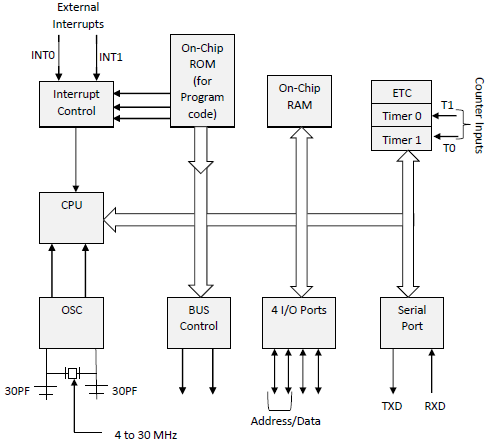
Microcontrollers - 8051 Architecture
8051 microcontroller is designed by Intel in 1981. It is an 8-bit microcontroller. It is built with 40 pins DIP (dual inline package), 4kb of ROM storage and 128 bytes of RAM storage, 2 16-bit timers. It consists of are four parallel 8-bit ports, which are programmable as well as addressable as per the requirement. An on-chip crystal oscillator is integrated in the microcontroller having crystal frequency of 12 MHz.
Let us now discuss the architecture of 8051 Microcontroller.
In the following diagram, the system bus connects all the support devices to the CPU. The system bus consists of an 8-bit data bus, a 16-bit address bus and bus control signals. All other devices like program memory, ports, data memory, serial interface, interrupt control, timers, and the CPU are all interfaced together through the system bus.