- Home
- Introduction
- Performance Characteristics
- Measurement Errors
- Measuring Instruments
- DC Voltmeters
- AC Voltmeters
- Other AC Voltmeters
- DC Ammeters
- AC Ammeter
- OHMMeters
- MultiMeter
- Signal Generators
- Wave Analyzers
- Spectrum Analyzers
- Basics of Oscilloscopes
- Special Purpose Oscilloscopes
- Lissajous Figures
- CRO Probes
- Bridges
- DC Bridges
- AC Bridges
- Other AC Bridges
- Transducers
- Active Transducers
- Passive Transducers
- Measurement Of Displacement
- Data Acquisition Systems
CRO Probes
We can connect any test circuit to an oscilloscope through a probe. As CRO is a basic oscilloscope, the probe which is connected to it is also called CRO probe.
We should select the probe in such a way that it should not create any loading issues with the test circuit. So that we can analyze the test circuit with the signals properly on CRO screen.
CRO probes should have the following characteristics.
- High impedance
- High bandwidth
The block diagram of CRO probe is shown in below figure.
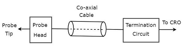
As shown in the figure, CRO probe mainly consists of three blocks. Those are probe head, co-axial cable and termination circuit. Co-axial cable simply connects the probe head and termination circuit.
Types of CRO Probes
CRO probes can be classified into the following two types.
- Passive Probes
- Active Probes
Now, let us discuss about these two types of probes one by one.
Passive Probes
If the probe head consists of passive elements, then it is called passive probe. The circuit diagram of passive probe is shown in below figure.
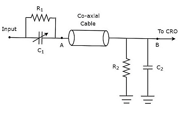
As shown in the figure, the probe head consists of a parallel combination of resistor, $R_{1}$ and a variable capacitor, $C_{1}$. Similarly, the termination circuit consists of a parallel combination of resistor, $R_{2}$ and capacitor, $C_{2}$.
The above circuit diagram is modified in the form of bridge circuit and it is shown in below figure.
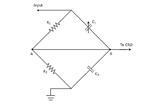
We can balance the bridge, by adjusting the value of variable capacitor, $c_{1}$. We will discuss the concept of bridges in the following chapters. For the time being, consider the following balancing condition of AC bridge.
$$Z_{1}Z_{4}=Z_{2}Z_{3}$$
Substitute, the impedances $Z_{1},Z_{2}, Z_{3}$ and $Z_{4}$ as $R_{1},\frac{1}{j\omega C_{1}}, R_{2}$ and $\frac{1}{j\omega C_{2}}$ respectively in above equation.
$$R_{1}\left ( \frac{1}{j \omega C_{2}} \right )=\left ( \frac{1}{j \omega C_{1}} \right )R_{2}$$
$\Rightarrow R_{1} C_{1}=R_{2} C_{2}$Equation 1
By voltage division principle, we will get the voltage across resistor, $R_{2}$ as
$$V_{0}=V_{i}\left ( \frac{R_{2}}{R_{1}+R_{2}} \right )$$
attenuation factor is the ratio of input voltage, $V_{i}$ and output voltage, $V_{0}$. So, from above equation we will get the attenuation factor, $\alpha$ as
$$\alpha = \frac{V_{i}}{V_{0}}=\frac{R_{1}+R_{2}}{R_{2}}$$
$\Rightarrow \alpha = 1+\frac{R_{1}}{R_{2}}$
$\Rightarrow \alpha-1 = \frac{R_{1}}{R_{2}}$
$\Rightarrow R_{1}= \left ( \alpha-1 \right )R_{2}$Equation 2
From Equation 2, we can conclude that the value of $R_{1}$ is greater than or equal to the value of 2 for integer values of$\:\alpha > 1$.
Substitute Equation 2 in Equation 1.
$$\left ( \alpha-1 \right )R_{2}C_{1}=R_{2}C_{2}$$
$\Rightarrow \left ( \alpha-1 \right )C_{1} =C_{2}$
$\Rightarrow C_{1}=\frac{C_{2}}{\left ( \alpha-1 \right )}$Equation 3
From Equation 3, we can conclude that the value of $C_{1}$ is less than or equal to the value of $C_{2}$ for integer values of $\alpha >1$
Example
Let us find the values of $R_{1}$ and $C_{1}$ of a probe having an attenuation factor,$\alpha$ as 10. Assume, $R_{2}=1 M \Omega$ and $C_{2}=18pF$.
Step1 − We will get the value of $R_{1}$ by substituting the values of $\alpha$ and $R_{2}$ in Equation 2.
$$ R_{1}=\left ( 10-1 \right )\times 1 \times 10^{6}$$
$$\Rightarrow R_{1}=9 \times 10^{6}$$
$$\Rightarrow R_{1}=9 M\Omega$$
Step 2 − We will get the value of $C_{1}$ by substituting the values of $\alpha$ and $C_{2}$ in Equation 3.
$$C_{1}=\frac{18\times10^{-12}}{\left ( 10-1 \right )}$$
$$\Rightarrow C_{1}=2 \times 10^{-12}$$
$$\Rightarrow C_{1}=2 pF$$
Therefore, the values of $R_{1}$ and $C_{1}$ of a probe will be $9M\Omega$ and $2pF$ respectively for the given specifications.
Active Probes
If the probe head consists of active electronic components, then it is called active probe. The block diagram of active probe is shown in below figure.
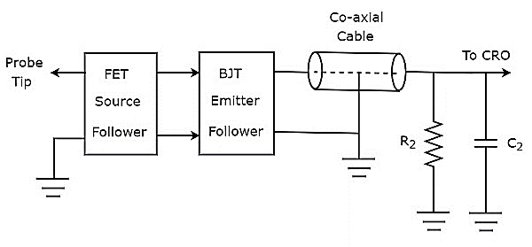
As shown in the figure, the probe head consists of a FET source follower in cascade with BJT emitter follower. The FET source follower provides high input impedance and low output impedance. Whereas, the purpose of BJT emitter follower is that it avoids or eliminates the impedance mismatching.
The other two parts, such as co-axial cable and termination circuit remain same in both active and passive probes.
