- Linear Integrated Circuits Applications
- Home
- Basics of Integrated Circuits Applications
- Basics Operational Amplifier
- Op-Amp applications
- Arithmetic Circuits
- Differentiator & Integrator
- Converters Of Electrical Quantities
- Comparators
- Log & Anti-Log Amplifiers
- Rectifiers
- Clippers
- Clampers
- Active Filters
- Sinusoidal Oscillators
- Waveform Generators
- 555 Timer
- Phase Locked Loop Ic
- Voltage Regulators
- Data Converters
- Digital to Analog Converters
- DAC Example Problem
- Direct Type ADCs
- Indirect Type ADC
- Useful Resources
- Quick Guide
- Useful Resources
- Discussion
Direct Type ADCs
An Analog to Digital Converter (ADC) converts an analog signal into a digital signal. The digital signal is represented with a binary code, which is a combination of bits 0 and 1.
The block diagram of an ADC is shown in the following figure −
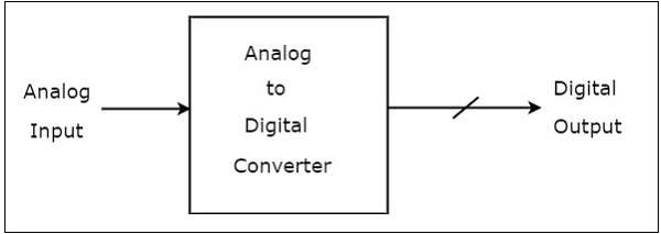
Observe that in the figure shown above, an Analog to Digital Converter (ADC) consists of a single analog input and many binary outputs. In general, the number of binary outputs of ADC will be a power of two.
There are two types of ADCs: Direct type ADCs and Indirect type ADC. This chapter discusses about the Direct type ADCs in detail.
If the ADC performs the analog to digital conversion directly by utilizing the internally generated equivalent digital (binary) code for comparing with the analog input, then it is called as Direct type ADC.
The following are the examples of Direct type ADCs −
- Counter type ADC
- Successive Approximation ADC
- Flash type ADC
This section discusses about these Direct type ADCs in detail.
Counter type ADC
A counter type ADC produces a digital output, which is approximately equal to the analog input by using counter operation internally.
The block diagram of a counter type ADC is shown in the following figure −
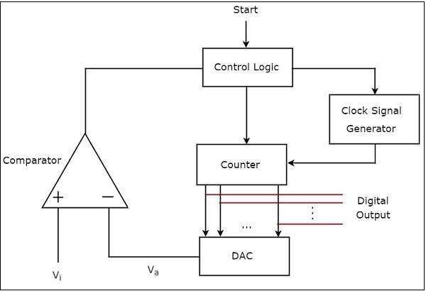
The counter type ADC mainly consists of 5 blocks: Clock signal generator, Counter, DAC, Comparator and Control logic.
The working of a counter type ADC is as follows −
The control logic resets the counter and enables the clock signal generator in order to send the clock pulses to the counter, when it received the start commanding signal.
The counter gets incremented by one for every clock pulse and its value will be in binary (digital) format. This output of the counter is applied as an input of DAC.
DAC converts the received binary (digital) input, which is the output of counter, into an analog output. Comparator compares this analog value,$V_{a}$ with the external analog input value $V_{i}$.
The output of comparator will be ‘1’ as long as 𝑉𝑖 is greater than. The operations mentioned in above two steps will be continued as long as the control logic receives ‘1’ from the output of comparator.
The output of comparator will be ‘0’ when $V_{i}$ is less than or equal to $V_{a}$. So, the control logic receives ‘0’ from the output of comparator. Then, the control logic disables the clock signal generator so that it doesn’t send any clock pulse to the counter.
At this instant, the output of the counter will be displayed as the digital output. It is almost equivalent to the corresponding external analog input value $V_{i}$.
Successive Approximation ADC
A successive approximation type ADC produces a digital output, which is approximately equal to the analog input by using successive approximation technique internally.
The block diagram of a successive approximation ADC is shown in the following figure
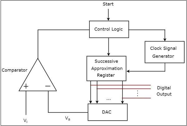
The successive approximation ADC mainly consists of 5 blocks− Clock signal generator, Successive Approximation Register (SAR), DAC, comparator and Control logic.
The working of a successive approximation ADC is as follows −
The control logic resets all the bits of SAR and enables the clock signal generator in order to send the clock pulses to SAR, when it received the start commanding signal.
The binary (digital) data present in SAR will be updated for every clock pulse based on the output of comparator. The output of SAR is applied as an input of DAC.
DAC converts the received digital input, which is the output of SAR, into an analog output. The comparator compares this analog value $V_{a}$ with the external analog input value $V_{i}$.
The output of a comparator will be ‘1’ as long as $V_{i}$ is greater than $V_{a}$. Similarly, the output of comparator will be ‘0’, when $V_{i}$ is less than or equal to $V_{a}$.
The operations mentioned in above steps will be continued until the digital output is a valid one.
The digital output will be a valid one, when it is almost equivalent to the corresponding external analog input value $V_{i}$.
Flash type ADC
A flash type ADC produces an equivalent digital output for a corresponding analog input in no time. Hence, flash type ADC is the fastest ADC.
The circuit diagram of a 3-bit flash type ADC is shown in the following figure −
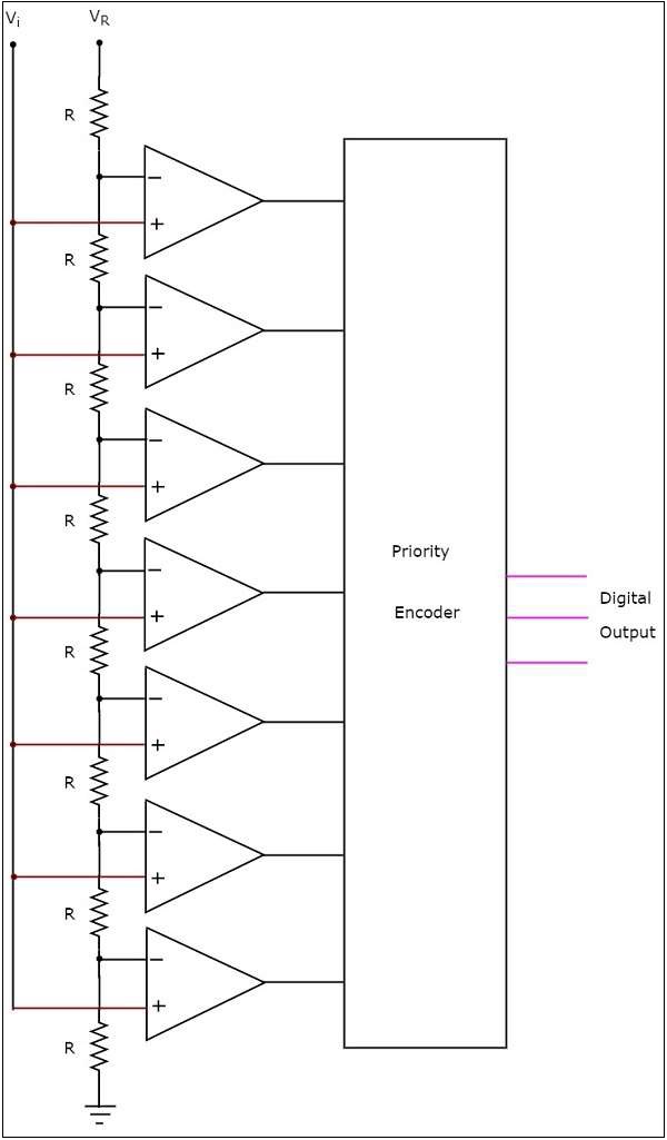
The 3-bit flash type ADC consists of a voltage divider network, 7 comparators and a priority encoder.
The working of a 3-bit flash type ADC is as follows.
The voltage divider networkcontains 8 equal resistors. A reference voltage $V_{R}$ is applied across that entire network with respect to the ground. The voltage drop across each resistor from bottom to top with respect to ground will be the integer multiples (from 1 to 8) of $\frac{V_{R}}{8}$.
The external input voltage $V_{i}$ is applied to the non-inverting terminal of all comparators. The voltage drop across each resistor from bottom to top with respect to ground is applied to the inverting terminal of comparators from bottom to top.
At a time, all the comparators compare the external input voltage with the voltage drops present at the respective other input terminal. That means, the comparison operations take place by each comparator parallelly.
The output of the comparator will be ‘1’ as long as $V_{i}$ is greater than the voltage drop present at the respective other input terminal. Similarly, the output of comparator will be ‘0’, when, $V_{i}$ is less than or equal to the voltage drop present at the respective other input terminal.
All the outputs of comparators are connected as the inputs of priority encoder.This priority encoder produces a binary code (digital output), which is corresponding to the high priority input that has ‘1’.
Therefore, the output of priority encoder is nothing but the binary equivalent (digital output) of external analog input voltage, $V_{i}$.
The flash type ADC is used in the applications where the conversion speed of analog input into digital data should be very high.