- Digital Circuits Tutorial
- Home
- Number Systems
- Base Conversions
- Binary Numbers Representation
- Signed Binary Arithmetic
- Codes
- Error Detection & Correction Codes
- Boolean Algebra
- Canonical and Standard Forms
- K-Map Method
- Quine-McCluskey Tabular Method
- Logic Gates
- Two-Level Logic Realization
- Combinational Circuits
- Arithmetic Circuits
- Decoders
- Encoders
- Multiplexers
- De-Multiplexers
- Programmable Logic Devices
- Threshold Logic
- Sequential Circuits
- Latches
- Flip-Flops
- Conversion of Flip-Flops
- Shift Registers
- Application of Shift Registers
- Counters
- Finite State Machines
- Algorithmic State Machine Charts
- Digital Circuits Resources
- Digital Circuits - Quick Guide
- Digital Circuits - Useful Resources
- Digital Circuits - Discussion
Digital Combinational Circuits
Combinational circuits consist of Logic gates. These circuits operate with binary values. The output(s) of combinational circuit depends on the combination of present inputs. The following figure shows the block diagram of combinational circuit.
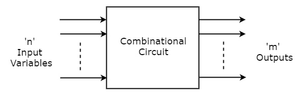
This combinational circuit has ‘n’ input variables and ‘m’ outputs. Each combination of input variables will affect the output(s).
Design procedure of Combinational circuits
Find the required number of input variables and outputs from given specifications.
Formulate the Truth table. If there are ‘n’ input variables, then there will be 2n possible combinations. For each combination of input, find the output values.
Find the Boolean expressions for each output. If necessary, simplify those expressions.
Implement the above Boolean expressions corresponding to each output by using Logic gates.
Code Converters
We have discussed various codes in the chapter named codes. The converters, which convert one code to other code are called as code converters. These code converters basically consist of Logic gates.
Example
Binary code to Gray code converter
Let us implement a converter, which converts a 4-bit binary code WXYZ into its equivalent Gray code ABCD.
The following table shows the Truth table of a 4-bit binary code to Gray code converter.
| Binary code WXYZ | WXYZ Gray code ABCD |
|---|---|
| 0000 | 0000 |
| 0001 | 0001 |
| 0010 | 0011 |
| 0011 | 0010 |
| 0100 | 0110 |
| 0101 | 0111 |
| 0110 | 0101 |
| 0111 | 0100 |
| 1000 | 1100 |
| 1001 | 1101 |
| 1010 | 1111 |
| 1011 | 1110 |
| 1100 | 1010 |
| 1101 | 1011 |
| 1110 | 1001 |
| 1111 | 1000 |
From Truth table, we can write the Boolean functions for each output bit of Gray code as below.
$$A=\sum m\left (8,9,10,11,12,13,14,15 \right )$$
$$B=\sum m\left (4,5,6,7,8,9,10,11 \right )$$
$$C=\sum m\left (2,3,4,5,10,11,12,13 \right )$$
$$D=\sum m\left (1,2,5,6,9,10,13,14 \right )$$
Let us simplify the above functions using 4 variable K-Maps.
The following figure shows the 4 variable K-Map for simplifying Boolean function, A.
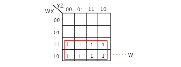
By grouping 8 adjacent ones, we got $A=W$.
The following figure shows the 4 variable K-Map for simplifying Boolean function, B.
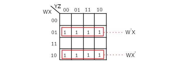
There are two groups of 4 adjacent ones. After grouping, we will get B as
$$B={W}'X+W{X}'=W\oplus X $$
Similarly, we will get the following Boolean functions for C & D after simplifying.
$$C={X}'Y+X{Y}'=X \oplus Y$$
$$D={Y}'Z+Y{Z}'=Y \oplus Z$$
The following figure shows the circuit diagram of 4-bit binary code to Gray code converter.
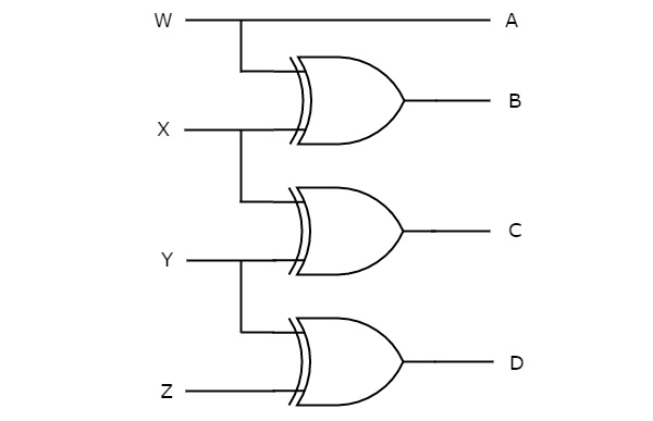
Since the outputs depend only on the present inputs, this 4-bit Binary code to Gray code converter is a combinational circuit. Similarly, you can implement other code converters.
Parity Bit Generator
There are two types of parity bit generators based on the type of parity bit being generated. Even parity generator generates an even parity bit. Similarly, odd parity generator generates an odd parity bit.
Even Parity Generator
Now, let us implement an even parity generator for a 3-bit binary input, WXY. It generates an even parity bit, P. If odd number of ones present in the input, then even parity bit, P should be ‘1’ so that the resultant word contains even number of ones. For other combinations of input, even parity bit, P should be ‘0’. The following table shows the Truth table of even parity generator.
| Binary Input WXY | Even Parity bit P |
|---|---|
| 000 | 0 |
| 001 | 1 |
| 010 | 1 |
| 011 | 0 |
| 100 | 1 |
| 101 | 0 |
| 110 | 0 |
| 111 | 1 |
From the above Truth table, we can write the Boolean function for even parity bit as
$$P={W}'{X}'Y+{W}'X{Y}'+W{X}'{Y}'+WXY$$
$\Rightarrow P={W}'\left ( {X}'Y+X{Y}' \right )+W\left ({X}'{Y}'+XY \right )$
$\Rightarrow P={W}'\left ( X \oplus Y \right )+W{\left (X \oplus Y \right )}'=W \oplus X \oplus Y$
The following figure shows the circuit diagram of even parity generator.
This circuit consists of two Exclusive-OR gates having two inputs each. First ExclusiveOR gate having two inputs W & X and produces an output W ⊕ X. This output is given as one input of second Exclusive-OR gate. The other input of this second Exclusive-OR gate is Y and produces an output of W ⊕ X ⊕ Y.
Odd Parity Generator
If even number of ones present in the input, then odd parity bit, P should be ‘1’ so that the resultant word contains odd number of ones. For other combinations of input, odd parity bit, P should be ‘0’.
Follow the same procedure of even parity generator for implementing odd parity generator. The circuit diagram of odd parity generator is shown in the following figure.
The above circuit diagram consists of Ex-OR gate in first level and Ex-NOR gate in second level. Since the odd parity is just opposite to even parity, we can place an inverter at the output of even parity generator. In that case, the first and second levels contain an ExOR gate in each level and third level consist of an inverter.
Parity Checker
There are two types of parity checkers based on the type of parity has to be checked. Even parity checker checks error in the transmitted data, which contains message bits along with even parity. Similarly, odd parity checker checks error in the transmitted data, which contains message bits along with odd parity.
Even parity checker
Now, let us implement an even parity checker circuit. Assume a 3-bit binary input, WXY is transmitted along with an even parity bit, P. So, the resultant word (data) contains 4 bits, which will be received as the input of even parity checker.
It generates an even parity check bit, E. This bit will be zero, if the received data contains an even number of ones. That means, there is no error in the received data. This even parity check bit will be one, if the received data contains an odd number of ones. That means, there is an error in the received data.
The following table shows the Truth table of an even parity checker.
| 4-bit Received Data WXYP | Even Parity Check bit E |
|---|---|
| 0000 | 0 |
| 0001 | 1 |
| 0010 | 1 |
| 0011 | 0 |
| 0100 | 1 |
| 0101 | 0 |
| 0110 | 0 |
| 0111 | 1 |
| 1000 | 1 |
| 1001 | 0 |
| 1010 | 0 |
| 1011 | 1 |
| 1100 | 0 |
| 1101 | 1 |
| 1110 | 1 |
| 1111 | 0 |
From the above Truth table, we can observe that the even parity check bit value is ‘1’, when odd number of ones present in the received data. That means the Boolean function of even parity check bit is an odd function. Exclusive-OR function satisfies this condition. Hence, we can directly write the Boolean function of even parity check bit as
$$E=W \oplus X \oplus Y \oplus P$$
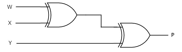
The following figure shows the circuit diagram of even parity checker.
This circuit consists of three Exclusive-OR gates having two inputs each. The first level gates produce outputs of $W \oplus X$ & $Y \oplus P$. The Exclusive-OR gate, which is in second level produces an output of $W \oplus X \oplus Y \oplus P$
Odd Parity Checker
Assume a 3-bit binary input, WXY is transmitted along with odd parity bit, P. So, the resultant word (data) contains 4 bits, which will be received as the input of odd parity checker.
It generates an odd parity check bit, E. This bit will be zero, if the received data contains an odd number of ones. That means, there is no error in the received data. This odd parity check bit will be one, if the received data contains even number of ones. That means, there is an error in the received data.
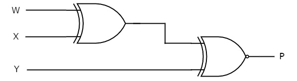
Follow the same procedure of an even parity checker for implementing an odd parity checker. The circuit diagram of odd parity checker is shown in the following figure.
The above circuit diagram consists of Ex-OR gates in first level and Ex-NOR gate in second level. Since the odd parity is just opposite to even parity, we can place an inverter at the output of even parity checker. In that case, the first, second and third levels contain two Ex-OR gates, one Ex-OR gate and one inverter respectively.