- Digital Circuits Tutorial
- Home
- Number Systems
- Base Conversions
- Binary Numbers Representation
- Signed Binary Arithmetic
- Codes
- Error Detection & Correction Codes
- Boolean Algebra
- Canonical and Standard Forms
- K-Map Method
- Quine-McCluskey Tabular Method
- Logic Gates
- Two-Level Logic Realization
- Combinational Circuits
- Arithmetic Circuits
- Decoders
- Encoders
- Multiplexers
- De-Multiplexers
- Programmable Logic Devices
- Threshold Logic
- Sequential Circuits
- Latches
- Flip-Flops
- Conversion of Flip-Flops
- Shift Registers
- Application of Shift Registers
- Counters
- Finite State Machines
- Algorithmic State Machine Charts
- Digital Circuits Resources
- Digital Circuits - Quick Guide
- Digital Circuits - Useful Resources
- Digital Circuits - Discussion
Digital Circuits - Latches
There are two types of memory elements based on the type of triggering that is suitable to operate it.
- Latches
- Flip-flops
Latches operate with enable signal, which is level sensitive. Whereas, flip-flops are edge sensitive. We will discuss about flip-flops in next chapter. Now, let us discuss about SR Latch & D Latch one by one.
SR Latch
SR Latch is also called as Set Reset Latch. This latch affects the outputs as long as the enable, E is maintained at ‘1’. The circuit diagram of SR Latch is shown in the following figure.
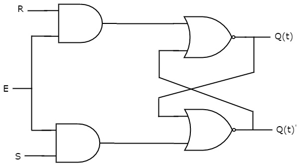
This circuit has two inputs S & R and two outputs Q(t) & Q(t)’. The upper NOR gate has two inputs R & complement of present state, Q(t)’ and produces next state, Q(t+1) when enable, E is ‘1’.
Similarly, the lower NOR gate has two inputs S & present state, Q(t) and produces complement of next state, Q(t+1)’ when enable, E is ‘1’.
We know that a 2-input NOR gate produces an output, which is the complement of another input when one of the input is ‘0’. Similarly, it produces ‘0’ output, when one of the input is ‘1’.
If S = 1, then next state Q(t + 1) will be equal to ‘1’ irrespective of present state, Q(t) values.
If R = 1, then next state Q(t + 1) will be equal to ‘0’ irrespective of present state, Q(t) values.
At any time, only of those two inputs should be ‘1’. If both inputs are ‘1’, then the next state Q(t + 1) value is undefined.
The following table shows the state table of SR latch.
| S | R | Q(t + 1) |
|---|---|---|
| 0 | 0 | Q(t) |
| 0 | 1 | 0 |
| 1 | 0 | 1 |
| 1 | 1 | - |
Therefore, SR Latch performs three types of functions such as Hold, Set & Reset based on the input conditions.
D Latch
There is one drawback of SR Latch. That is the next state value can’t be predicted when both the inputs S & R are one. So, we can overcome this difficulty by D Latch. It is also called as Data Latch. The circuit diagram of D Latch is shown in the following figure.
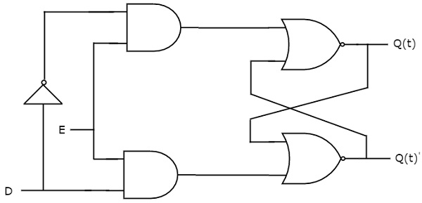
This circuit has single input D and two outputs Q(t) & Q(t)’. D Latch is obtained from SR Latch by placing an inverter between S amp;& R inputs and connect D input to S. That means we eliminated the combinations of S & R are of same value.
If D = 0 → S = 0 & R = 1, then next state Q(t + 1) will be equal to ‘0’ irrespective of present state, Q(t) values. This is corresponding to the second row of SR Latch state table.
If D = 1 → S = 1 & R = 0, then next state Q(t + 1) will be equal to ‘1’ irrespective of present state, Q(t) values. This is corresponding to the third row of SR Latch state table.
The following table shows the state table of D latch.
| D | Q(t + 1) |
|---|---|
| 0 | 0 |
| 1 | 1 |
Therefore, D Latch Hold the information that is available on data input, D. That means the output of D Latch is sensitive to the changes in the input, D as long as the enable is High.
In this chapter, we implemented various Latches by providing the cross coupling between NOR gates. Similarly, you can implement these Latches using NAND gates.