
- Semiconductor Devices - Home
- Introduction
- Atomic Combinations
- Conduction in Solid Materials
- Conductivity & Mobility
- Types of Semiconductor
- Doping in Semiconductors
- Junction Diodes
- Depletion Zone
- Barrier Potential
- Junction Biasing
- Leakage Current
- Diode Characteristics
- Light Emitting Diode
- Zener Diode
- Photo Diode
- Photovoltaic Cells
- Varactor Diode
- Bipolar Transistors
- Construction of a Transistor
- Transistor Biasing
- Configuration of Transistors
- Field Effect Transistors
- JFET Biasing
- Semiconductor Devices - MOSFET
- Operational Amplifiers
- Practical Op-Amps
- Semiconductor Devices - Integrator
- Differentiator
- Oscillators
- Feedback & Compensation
- Semiconductor Devices - Quick Guide
- Semiconductor Devices - Resources
- Semiconductor Devices - Discussion
Semiconductor Devices - Quick Guide
Semiconductor Devices - Introduction
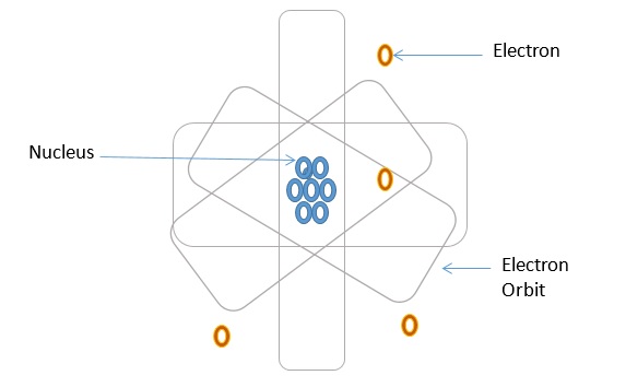
It is widely seen that the distance of a nucleus from the electron of a particular atom is not equal. Normally, electrons rotate in a well-defined orbit. A particular number of electrons can only hold by outer shell or orbit. The electrical conductivity of an atom is influenced mainly by the electrons of the outer shell. These electrons have a great deal to do with the electrical conductivity.
Conductors and Insulators
Electrical conduction is the result of irregular or uncontrolled movement of electrons. These movements cause certain atoms to be good electrical conductors. A material with such type of atoms has many free electrons in its outer shell or orbit.
Comparatively, an insulating material has a relatively small number of free electrons. Consequently, the outer shell electrons of insulators tend to hold their place firmly and hardly allow any current to flow through it. Therefore, in an insulating material, very little electrical conductivity takes place.
Semiconductors
In between conductors and insulators, there is a third classification of atoms (material) known as semiconductors. Generally, the conductivity of a semiconductor lies in between the conductivities of metals and insulators. However, at absolute zero temperature, the semiconductor also acts like a perfect insulator.
Silicon and germanium are the most familiar semiconductor elements. Copper oxide, cadmium-sulfide, and gallium arsenide are some other semiconductor compounds that are frequently used. These kinds of material are generally classified as type IVB elements. Such atoms have four valence electrons. If they can give up four valence electrons, stability can be accomplished. It can also be achieved by accepting four electrons.
Stability of an Atom
The concept of stability of an atom is an important factor in the status of semiconductor materials. The maximum number of electrons in the valence band is 8. When there are exactly 8 electrons in the valence band, it can be said that the atom is stable. In a stable atom, the bonding of valence electrons is very rigid. These types of atoms are excellent insulators. In such atoms, free electrons are not available for electrical conductivity.
Examples of stabilized elements are gases such as Argon, Xenon, Neon, and Krypton. Due to their property, these gases cannot be mixed with other material and are generally known as inert gases.
If the number of valence electrons in the outer shell is less than 8, then the atom is said to be unstable i.e., the atoms having fewer than 8 valence electrons are unstable. They always try to borrow or donate electrons from the neighboring atoms to become stable. Atoms in the outer shell with 5, 6, or 7 valence electrons tend to borrow electrons from other atoms to seek stability, while atoms with one, two, or three valence electrons tend to release these electrons to other nearby atoms.
Atomic Combinations
Anything that has weight is matter. As per the theory of atom, all matter, whether it is solid, liquid, or gas is composed of atoms. An atom contains a central part called nucleus, which holds the neutrons and the protons. Normally, protons are positively charged particles and neutrons are neutrally charged particles. Electrons which are negatively charged particles are arranged in orbits around the nucleus in a way similar to the array of planets around the Sun. The following figure shows the composition of an atom.
Atoms of different elements are found to have different number of protons, neutrons, and electrons. To distinguish one atom from another or to classify the various atoms, a number which indicates the number of protons in the nucleus of a given atom, is assigned to the atoms of each identified element. This number is known as the atomic number of the element. The atomic numbers for some of the elements which are associated with the study of semiconductors are given in the following table.
| Element | Symbol | Atomic Number |
|---|---|---|
| Silicon | Si | 14 |
| Germanium | Ge | 32 |
| Arsenic | As | 33 |
| Antimony | Sb | 51 |
| Indium | In | 49 |
| Gallium | Ga | 31 |
| Boron | B | 5 |
Normally, an atom has an equal number of protons and planetary electrons to maintain its net charge at zero. Atoms frequently combine to form stabilized molecules or compounds through their available valence electrons.
The process of combining of free valence electrons is generally called bonding. Following are the different kinds of bonding that takes place in atom combinations.
- Ionic bonding
- Covalent bonding
- Metallic bonding
Let us now discuss in detail about these atomic bondings.
Ionic Bonding
Each atom is seeking stability when the atoms bond together to form molecules. When the valence band contains 8 electrons, it is said to be a stabilized condition. When the valence electrons of one atom combine with those of another atom to become stable, it is called ionic bonding.
If an atom has more than 4 valence electrons in the outer shell it is seeking additional electrons. Such atom is often called an acceptor.
If any atom holds less than 4 valence electrons in the outer shell, they try to move out from these electrons. These atoms are known as donors.
In ionic bonding, donor and acceptor atoms frequently combine together and the combination becomes stabilized. Common salt is a common example of ionic bonding.
The following figures illustrate an example of independent atoms and ionic bonding.
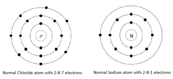
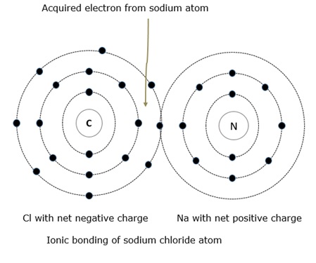
It can be seen in the above figure that the sodium (Na) atom donates its 1 valence electron to the chloride (Cl) atom which has 7 valence electrons. The chloride atom immediately becomes overbalanced negatively when it obtains the extra electron and this causes the atom to become a negative ion. While on the other hand, the sodium atom loses its valence electron and the sodium atom then becomes a positive ion. As we know unlike charges attract, the sodium and chloride atoms are bound together by an electrostatic force.
Covalent Bonding
When the valence electrons of neighboring atoms are shared with other atoms, covalent bonding takes place. In covalent bonding, ions are not formed. This is a unique dissimilarity in covalent bonding and ionic bonding.
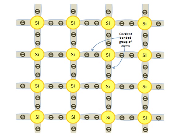
When an atom contains four valence electrons in the outer shell, it can share one electron with four neighboring atoms. A covalent force is established between the two linking electrons. These electrons alternately shift orbits between the atoms. This covalent force bonds the individual atoms together. An illustration of covalent bonding is shown in the following figures.
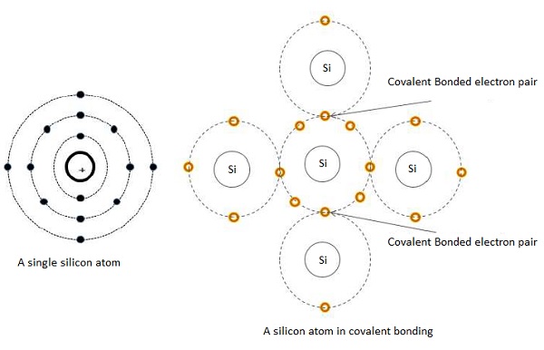
In this arrangement, only the nucleus and valence electrons of each atom are shown. Electron pair are created due to individual atoms are bonded together. In this case, five atoms are needed to complete the bonding action. The bonding process widens out in all directions. Each atom is now linked together in a lattice network and a crystal structure is formed by this lattice network.
Metallic Bonding
The third type of bonding generally occurs in good electrical conductors and it is called as metallic bonding. In metallic bonding, an electrostatic force exists between the positive ions and electrons. For example, the valence band of copper has one electron in its outer shell. This electron has a tendency to roam around the material between different atoms.
When this electron leaves one atom, it instantly enters the orbit of another atom. The process is repetitive on a nonstop basis. An atom becomes a positive ion when an electron leaves it. This is a random process. It means that one electron is always linked with an atom. It does not mean that the electron is associated with one particular orbit. It is always roaming in different orbits. As a consequence, all atoms are likely to share all the valence electrons.
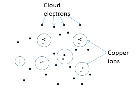
Electrons hang around in a cloud that covers the positive ions. This hovering cloud bonds the electrons randomly to the ions. The following figure shows an example of the metallic bonding of copper.
Conduction in Solid Materials
The number of electrons in the outer ring of an atom is still the reason for the difference between conductors and insulators. As we know, solid materials are primarily used in electrical devices to accomplish electron conduction. These materials can be separated into conductors, semiconductors, and insulators.
However, conductors, semiconductors, and insulators are differentiated by energy-level diagrams. The amount of energy needed to cause an electron to leave its valence band and go into conduction will be accounted here. The diagram is a composite of all atoms within the material. Energy-level diagrams of insulators, semiconductors, and conductors are shown in the following figure.
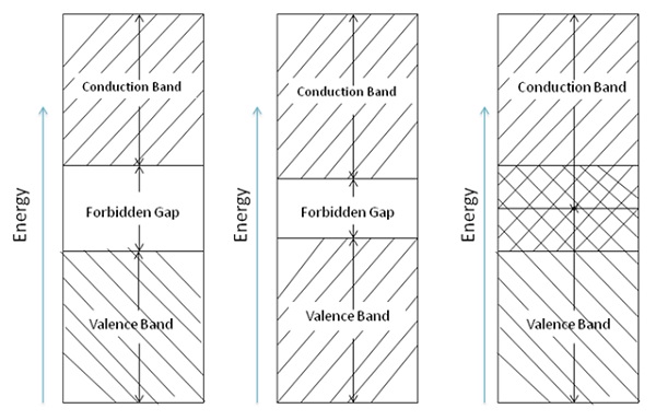
Valence Band
The bottom portion is the valence band. It represents the energy levels closest to the nucleus of the atom and the energy levels in the valance band hold the correct number of electron necessary to balance the positive charge of the nucleus. Thus, this band is called the filled band.
In the valence band, electrons are tightly bound to the nucleus. Moving upward in the energy level, the electrons are more lightly bound in each succeeding level toward the nucleus. It is not easy to disturb the electrons in the energy levels closer to the nucleus, as their movement requires larger energies and each electron orbit has a distinct energy level.
Conduction Band
The top or outermost band in the diagram is called the conduction band. If an electron has an energy level, which lies within this band, and is comparatively free to move around in the crystal, then it conducts electric current.
In semiconductor electronics, we are concerned mostly in the valence and conduction bands. Following are some basic information about it −
The valence band of each atom shows the energy levels of the valence electrons in the outer shell.
A definite amount of energy must be added to the valence electrons to cause them to go into the conduction band.
Forbidden Gap
The valence and conduction bands are separated by a gap, wherever exists, called forbidden gap. To cross the forbidden gap a definite amount of energy is needed. If it is insufficient, electrons are not released for conduction. Electrons will remain in the valence band till they receive additional energy to cross the forbidden gap.
The conduction status of a particular material can be indicated by the width of the forbidden gap. In atomic theory, the width of the gap is expressed in electron volts (eV). An electron volt is defined as the amount of energy gained or lost when an electron is subjected to a potential difference of 1 V. The atoms of each element have a dissimilar energy-level value that allows conduction.
Note that the forbidden region of an insulator is relatively wide. To cause an insulator to go into conduction will require a very large amount of energy. For example, Thyrite.
If insulators are operated at high temperatures, the increased heat energy causes the electrons of the valence band to move into the conduction band.
As it is clear from the energy band diagram, the forbidden gap of a semiconductor is much smaller than that of an insulator. For example, silicon needs to gain 0.7 eV of energy to go into the conduction band. At room temperature, the addition of heat energy may be sufficient to cause conduction in a semiconductor. This particular characteristic is of great importance in solid-state electronic devices.
In case of a conductor, the conduction band and the valence band partly overlaps one another. In a sense, there is no forbidden gap. Therefore, the electrons of valence band are able to release to become free electrons. Normally at normal room temperature little electrical conduction takes place within the conductor.
Conductivity & Mobility
As discussed earlier, there may be one or more free electrons per atom which moves all the way through the interior of the metal under the influence of an applied field.
The following figure shows charge distribution within a metal. It is known as the electron-gas description of a metal.
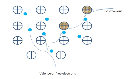
The hashed region represents the nucleus with a positive charge. The blue dots represent the valence electrons in the outer shell of an atom. Basically, these electrons do not belong to any specific atom and as a result, they have lost their individual identity and roam freely atom to atom.
When the electrons are in an uninterrupted motion, the direction of transportation is changed at each collision with the heavy ions. This is based on electron-gas theory of a metal. The average distance between collisions is called the mean free path. The electrons, passing through a unit area, in the metal in the opposite direction in a given time, on a random basis, makes the average current zero.
Types of Semiconductor
When voltage is applied to semiconductor devices, electron current flows toward the positive side of the source and holes current flows towards the negative side of the source. Such a situation occurs only in a semiconductor material.
Silicon and Germanium are the most common semiconductor materials. Generally, the conductivity of a semiconductor lies in between the conductivities of metals and insulators.
Germanium as a Semiconductor
Following are some important points about Germanium −
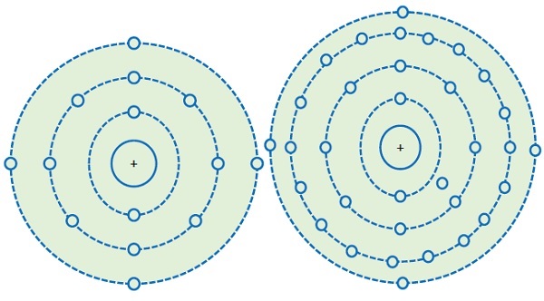
There are four electrons in the outermost orbit of germanium. In bonds, atoms are shown with their outer electrons only.
The germanium atoms will share valence electrons in a covalent bond. This is shown in the following figure. Germanium are the ones that are associated with the covalent bonding. The crystalline form of germanium is called the crystal lattices. This type of structure has the atoms arranged in the way as shown in the following figure.
In such an arrangement, the electrons are in a very stable state and thus are less appropriate to be associated with conductors. In the pure form, germanium is an insulating material and is called as an intrinsic semiconductor.
The following figure shows the atomic structures of Silicon and Germanium.
Silicon as a Semiconductor
Semiconductor devices also use silicon in the manufacturing of various electronic components. The atomic structure of silicon and germanium is shown in the above figure. The crystal lattice structure of silicon is similar to that of Germanium.
Following are some of the important points about Silicon −
It has four electrons in its outermost shell like germanium.
In pure form, it is of no use as a semiconductor device.
A desired amount of conductivity can be obtained by adding up of impurities.
Adding up of impurity must be done carefully and in a controlled environment.
Depending on the type of impurity added, it will create either an excess or a deficit of electrons.
The following figure shows the intrinsic crystal of Silicon.
Doping in Semiconductors
Pure Silicon or Germanium are rarely used as semiconductors. Practically usable semiconductors must have controlled quantity of impurities added to them. Addition of impurity will change the conductor ability and it acts as a semiconductor. The process of adding an impurity to an intrinsic or pure material is called doping and the impurity is called a dopant. After doping, an intrinsic material becomes an extrinsic material. Practically only after doping these materials become usable.
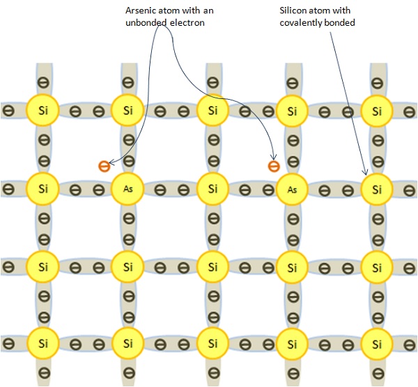
When an impurity is added to silicon or germanium without modifying the crystal structure, an N-type material is produced. In some atoms, electrons have five electrons in their valence band such as arsenic (As) and antimony (Sb). Doping of silicon with either impurity must not change the crystal structure or the bonding process. The extra electron of impurity atom does not take part in a covalent bonding. These electrons are loosely held together by their originator atoms. The following figure shows alteration of silicon crystal with the addition of an impurity atom.
Effect of Doping on N-type Material
The effect of doping on an N-type material is as follows −
On addition of Arsenic to pure Silicon, the crystal becomes an N-type material.
Arsenic atom has additional electrons or negative charges that do not take part in the process of covalent bonding.
These impurities give up or donate, one electron to the crystal and they are referred to as donor impurities.
An N-type material has extra or free electrons than an intrinsic material.
An N-type material is not negatively charged. Actually all of its atoms are all electrically neutral.
These extra electrons do not take part in the covalent bonding process. They are free to move about through the crystal structure.
An N-type extrinsic silicon crystal will go into conduction with only 0.005eV of energy applied.
Only 0.7eV is required to move electrons of intrinsic crystal from the valence band into the conduction band.
Normally, electrons are considered to be the majority current carriers in this type of crystal and holes are the minority current carriers. The quantity of donor material added to Silicon finds out the number of majority current carriers in its structure.
The number of electrons in an N-type silicon is many times greater than the electron-hole pairs of intrinsic silicon. At room temperature, there is a firm difference in the electrical conductivity of this material. There are abundant current carriers to take part in the current flow. The flow of current is achieved mostly by electrons in this type of material. Therefore, an extrinsic material becomes a good electrical conductor.
Effect of Doping on P-type Material
The effect of doping on a P-type material is as follows −
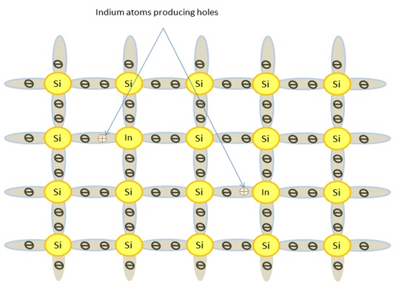
When Indium (In) or Gallium (Ga) is added to pure silicon, a P-type material is formed.
This type of dopant material has three valence electrons. They are eagerly looking for a fourth electron.
In P type material, each hole can be filled with an electron. To fill this hole area, very less energy is required by electrons from the neighboring covalent bonded groups.
Silicon is typically doped with doping material in the range of 1 to 106. This means that P material will have much more holes than the electron-hole pairs of pure silicon.
At room temperature, there is a very determined characteristic difference in the electrical conductivity of this material.
The following figure shows how the crystal structure of Silicon is altered when doped with an acceptor element in this case, Indium. A piece of P material is not positively charged. Its atoms are primarily all electrically neutral.
There are, however, holes in the covalent structure of many atom groups. When an electron moves in and fills a hole, the hole becomes void. A new hole is created in the bonded group where the electron left. Hole movement in effect is the result of electron movement. A P-type material will go into conduction with only 0.05 eV of energy applied.
The above figure shows how a P-type crystal will respond when connected to a voltage source. Note that there are larger numbers of holes than electrons. With voltage applied, the electrons are attracted to the positive battery terminal.
Holes move, in a sense, toward the negative battery terminal. An electron is picked up at this point. The electron immediately fills a hole. The hole then becomes void. At the same time, an electron is pulled from the material by the positive battery terminal. Holes therefore move toward the negative terminal due to electrons shifting between different bonded groups. With energy applied, hole flow is continuous.
Semiconductor Devices - Junction Diodes
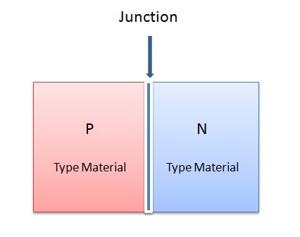
A crystal structure made of P and N materials is generally known as junction diode. It is generally regarded as a two-terminal device. As shown in the following diagram one terminal is attached to P-type material and the other to N-type material.
The common bond point where these materials are connected is called a junction. A junction diode allows current carriers to flow in one direction and obstruct the flow of current in the reverse direction.
The following figure shows the crystal structure of a junction diode. Take a look at the location of the P type and N type materials with respect to the junction. The structure of crystal is continuous from one end to the other. The junction acts only as a separating point that represents the end of one material and the beginning of the other. Such structure allows electrons to move thoroughly in the entire structure.
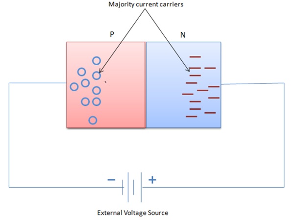
The following diagram shows two portions of semiconductor substance before they are shaped into a P-N junction. As specified, each part of material has majority and minority current carriers.
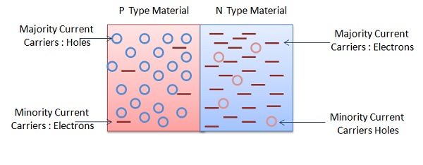
The quantity of carrier symbols shown in each material indicates the minority or majority function. As we know electrons are the majority carriers in the N type material and holes are the minority carriers. In P type material, holes are the majority carriers and electrons are in the minority.
Semiconductor Devices - Depletion Zone
Initially, when a junction diode is formed, there is a unique interaction between current carriers. In N type material, the electrons move readily across the junction to fill holes in the P material. This act is commonly called diffusion. Diffusion is the result of high accumulation of carriers in one material and a lower gathering in the other.
Generally, the current carriers which are near to the junction only takes part in the process of diffusion. Electrons departing the N material cause positive ions to be generated in their place. While entering the P material to fill holes, negative ions are created by these electrons. As a result, each side of the junction contains a large number of positive and negative ions.
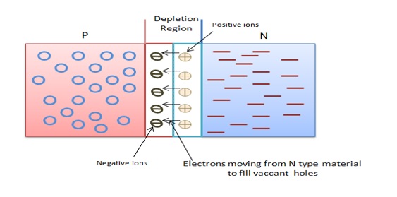
The area where these holes and electrons become depleted is generally known by the term depletion region. It is an area where there is lack of majority current carriers. Normally, a depletion region is developed when P-N junction is formed. The following figure shows the depletion region of a junction diode.
Semiconductor Devices - Barrier Potential
N-type and P-type material are considered as electrically neutral before they are joined together at a common junction. However, after joining diffusion takes place instantaneously, as electrons cross the junction to fill holes causing negative ions to emerge in the P material, this action causes the nearby area of the junction to take on a negative charge. Electrons departing the N material causes it to generate positive ions.
All this process, in turn, causes the N side of the junction to take on a net positive charge. This particular charge creation tends to force the remaining electrons and holes away from the junction. This action makes it somewhat hard for other charge carriers to diffuse across the junction. As a result, the charge is built up or barrier potential emerges across the junction.
As shown in the following figure. The resultant barrier potential has a small battery connected across the P-N junction. In the given figure observe the polarity of this potential barrier with respect to P and N material. This voltage or potential will exist when the crystal is not connected to an external source of energy.
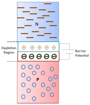
The barrier potential of germanium is approximately 0.3 V, and of silicon is 0.7 V. These values cannot be measured directly and appears across the space charge region of the junction. In order to produce current conduction, the barrier potential of a P-N junction must be overcome by an external voltage source.
Semiconductor Devices - Junction Biasing
The term bias refers to the application of DC voltage to set up certain operating conditions. Or when an external source of energy is applied to a P-N junction it is called a bias voltage or simply biasing. This method either increases or decreases the barrier potential of the junction. As a result, the reduction of the barrier potential causes current carriers to return to the depletion region. Following two bias conditions are applied w.r.t. PN junctions.
Forward Biasing − An external voltage is added of the same polarity to the barrier potential, which causes an increase in the width of the depletion region.
Reverse Biasing − A PN junction is biased in such a way that the application of external voltage action prevents current carriers from entering the depletion region.
Forward Biasing
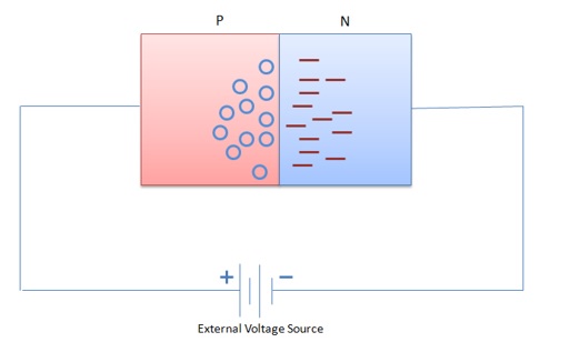
The following figure shows a forward biased PN junction diode with external voltage applied. You can see that the positive terminal of the battery is connected to the P material and the negative terminal of the battery is connected to the N material.
Following are the observations −
This bias voltage repels the majority current carriers of each P and N type material. As a result, large number of holes and electrons start appearing at the junction.
At the N-side of the junction, electrons move in to neutralize the positive ions in the depletion region.
On the P-side material, electrons are dragged from negative ions, which cause them to become neutral again. This means that forward biasing collapses the depletion region and hence the barrier potential too. It means that when P-N junction is forward biased, it will allow a continuous current flow.
The following figure shows the flow of current carriers of a forward-biased diode. A constant supply of electrons is available due to an external voltage source connected to the diode. The flow and direction of the current is shown by large arrows outside the diode in the diagram. Note that the electron flow and the current flow refers to the same thing.
Following are the observations −
Suppose electrons flow through a wire from the negative battery terminal to the N material. Upon entering this material, they flow immediately to the junction.
Similarly, on the other side an equal number of electrons are pulled from P side and are returned to the positive battery terminal. This action creates new holes and causes them to move toward the junction.
When these holes and electrons reach the junction they join together and effectively disappear. As a result, new holes and electrons emerge at the outer ends of the diode. These majority carriers are created on a continuous basis. This action continues as long as the external voltage source is applied.
When diode is forward biased it can be noticed that electrons flow through the entire structure of diode. This is common in N type material, whereas in the P material holes are the moving current carriers. Notice that the hole movement in one direction must begin by electron movement in the opposite direction. Therefore, the total current flow is the addition of holes and electrons flow through a diode.
Reverse Biasing
The following figure shows reverse biased PN junction diode with external voltage applied. You can see that the positive terminal of the battery is connected to the N material and the negative terminal of the battery is connected to the P material. Note that in such an arrangement, battery polarity is to oppose the material polarity of the diode so that dissimilar charges attract. Hence, majority charge carriers of each material are dragged away from the junction. Reverse biasing causes the diode to be nonconductive.
The following figure shows the arrangement of the majority current carriers in a reverse biased diode.
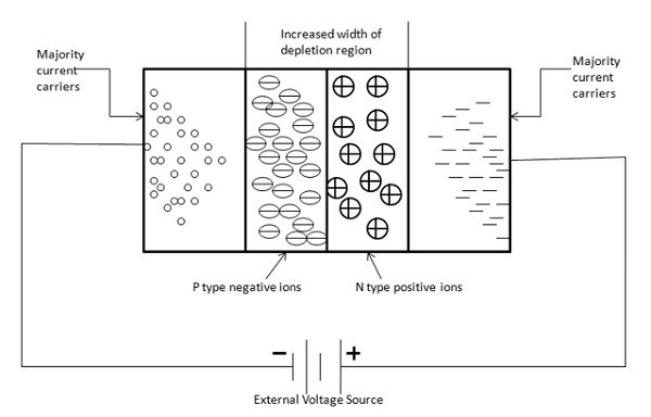
Following are the observations −
Due to circuit action electrons of the N material are pulled toward the positive battery terminal.
Each electron that moves or departs the diode causes a positive ion to emerge in its place. As a result, this causes an equivalent increase in the width of the depletion region on the N side of the junction.
The P side of the diode has a similar effect alike the N side. In this action, a number of electrons leave the negative battery terminal and enter the P type material.
These electrons then straight away move in and fill a number of holes. Each occupied hole then becomes a negative ion. These ions in turn are then repelled by the negative battery terminal and driven toward the junction. Due to this, there is an increase in the width of the depletion region on the P side of the junction.
The overall width of the depletion region directly depends on an external voltage source of a reverse-biased diode. In this case, the diode cannot efficiently support the current flow through the wide depletion region. As a result, the potential charge starts developing across the junction and increases until the barrier potential equals the external bias voltage. After this, the diode behaves as a nonconductor.
Semiconductor Devices - Leakage Current
An important conduction limitation of PN junction diode is leakage current. When a diode is reverse biased, the width of the depletion region increases. Generally, this condition is required to restrict the current carrier accumulation near the junction. Majority current carriers are primarily negated in the depletion region and hence the depletion region acts as an insulator. Normally, current carriers do not pass through an insulator.
It is seen that in a reverse-biased diode, some current flows through the depletion region. This current is called leakage current. Leakage current is dependent on minority current carriers. As we know that the minority carriers are electrons in the P type material and holes in the N type material.
The following figure shows how current carriers react when a diode is reverse biased.
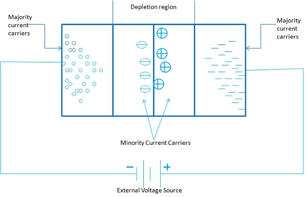
Following are the observations −
Minority carriers of each material are pushed through the depletion zone to the junction. This action causes a very small leakage current to occur. Generally, leakage current is so small that it can be considered as negligible.
Here, in case of leakage current, temperature plays an important role. The minority current carriers are mostly temperature dependent.
At room temperatures of 25C or 78F, there is negligible amount of minority carriers present in a reverse bias diode.
When the surrounding temperature rises, it causes significant increase in minority carrier creation and as a result it causes a corresponding increase in leakage current.
In all reverse-biased diodes, occurrence of leakage current is normal to some extent. In Germanium and Silicon diodes, leakage current is only of few microamperes and nanoamperes, respectively. Germanium is much more susceptible to temperature than silicon. For this reason, mostly Silicon is used in modern semiconductor devices.
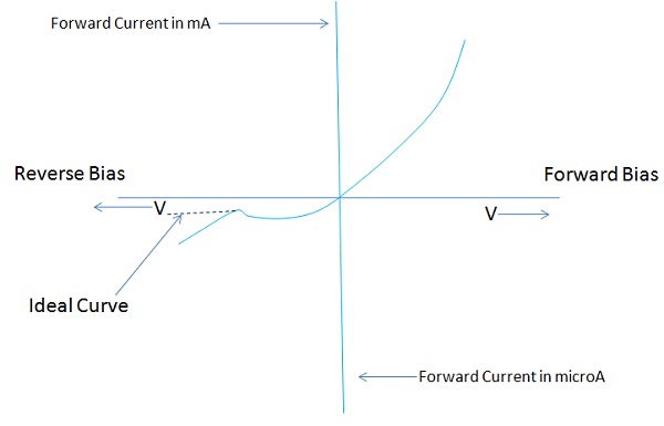
Diode Characteristics
There are diverse current scales for forward bias and reverse bias operations. The forward portion of the curve indicates that the diode conducts simply when the P-region is made positive and the N-region negative.
The diode conducts almost no current in the high resistance direction, i.e. when the Pregion is made negative and the N-region is made positive. Now the holes and electrons are drained away from the junction, causing the barrier potential to increase. This condition is indicated by the reverse current portion of the curve.
The dotted section of the curve indicates the ideal curve, which would result if it were not for avalanche breakdown. The following figure shows the static characteristic of a junction diode.
DIODE IV Characteristics
The forward and reverse current voltage (IV) characteristics of a diode are generally compared on a single characteristic curve. The figure depicted under the section Forward Characteristic shows that Forward Voltage and Reverse Voltage are usually plotted on the horizontal line of the graph.
Forward and reverse current values are shown on the vertical axis of the graph. Forward Voltage represented to the right and Reverse Voltage to the left. The point of beginning or zero value is at the center of the graph. Forward Current lengthens above the horizontal axis with Reverse Current extending downward.
The combined Forward Voltage and Forward Current values are located in the upper right part of the graph and Reverse Voltage and Reverse Current in the lower left corner. Different scales are normally used to display forward and reverse values.
Forward Characteristic
When a diode is forward biased it conducts current (IF) in forward direction. The value of IF is directly dependent on the amount of forward voltage. The relationship of forward voltage and forward current is called the ampere-volt, or IV characteristic of a diode. A typical diode forward IV characteristic is shown in the following figure.
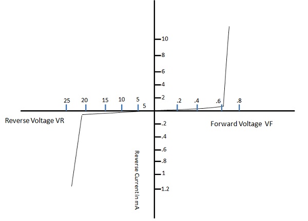
Following are the observations −
Forward Voltage is measured across the diode and Forward Current is a measure of current through the diode.
When the forward voltage across the diode equals 0V, forward current (IF) equals 0 mA.
When the value starts from the starting point (0) of the graph, if VF is progressively increased in 0.1-V steps, IF begins to rise.
When the value of VF is large enough to overcome the barrier potential of the P-N junction, a considerable increase in IF occurs. The point at which this occurs is often called the knee voltage VK. For germanium diodes, VK is approximately 0.3 V, and 0.7 V for silicon.
If the value of IF increases much beyond VK, the forward current becomes quite large.
This operation causes excessive heat to develop across the junction and can destroy a diode. To avoid this situation, a protective resistor is connected in series with the diode. This resistor limits the forward current to its maximum rated value. Normally, a currentlimiting resistor is used when diodes are operated in the forward direction.
Reverse Characteristic
When a diode is reverse biased, it conducts Reverse current that is usually quite small. A typical diode reverse IV characteristic is shown in the above figure.
The vertical reverse current line in this graph has current values expressed in microamperes. The amount of minority current carriers that take part in conduction of reverse current is quite small. In general, this means that reverse current remains constant over a large part of reverse voltage. When the reverse voltage of a diode is increased from the start, there is a very slight change in the reverse current. At the breakdown voltage (VBR) point, current increases very rapidly. The voltage across the diode remains reasonably constant at this time.
This constant-voltage characteristic leads to a number of applications of diode under reverse bias condition. The processes which are responsible for current conduction in a reverse-biased diode are called as Avalanche breakdown and Zener breakdown.
Diode Specifications
Like any other selection, selection of a diode for a specific application must be considered. Manufacturer generally provides this type of information. Specifications like maximum voltage and current ratings, usual operating conditions, mechanical facts, lead identification, mounting procedures, etc.
Following are some of the important specifications −
Maximum forward current (IFM) − The absolute maximum repetitive forward current that can pass through a diode.
Maximum reverse voltage (VRM) − The absolute maximum or peak reverse bias voltage that can be applied to a diode.
Reverse breakdown voltage (VBR) − The minimum steady-state reverse voltage at which breakdown will occur.
Maximum forward surge current (IFM-surge) − The maximum current that can be tolerated for a short interval of time. This current value is much greater than IFM.
Maximum reverse current (IR) − The absolute maximum reverse current that can be tolerated at device operating temperature.
Forward voltage (VF) − Maximum forward voltage drop for a given forward current at device operating temperature.
Power dissipation (PD) − The maximum power that the device can safely absorb on a continuous basis in free air at 25 C.
Reverse recovery time (Trr) − The maximum time that it takes the device to switch from on to off stat.
Important Terms
Breakdown Voltage − It is the minimum reverse bias voltage at which PN junction breaks down with sudden rise in reverse current.
Knee Voltage − It is the forward voltage at which the current through the junction starts to increase rapidly.
Peak Inverse Voltage − It is the maximum reverse voltage that can be applied to the PN junction, without damaging it.
Maximum Forward Rating − It is the highest instantaneous forward current that a PN junction can pass, without damaging it.
Maximum Power Rating − It is the maximum power that can be dissipated from the junction, without damaging the junction.
Light Emitting Diode
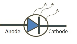
Light Emitting Diodes are directly or indirectly influencing our day-to-day activities. From the message display to LED TVs, everywhere these LEDs exist. It is basically a P-N junction diode that emits light when a forward current is allowed to pass through it. The following figure shows the logic symbol of an LED.
How Does a PN Junction Diode Emit Light?
LEDs are not made from Silicon or Germanium and elements like Gallium Arsenide (GaAs) and Gallium Phosphide (GaP). These materials are deliberately used as they emit light. Hence, when an LED is forward-biased, as usual electrons cross the junction and unite with holes.
This action causes electrons of N-type region to fall out of conduction and return to the valence band. In doing so, the energy possessed by each free electron is then released. A part of released energy emerges as heat and the rest of it is given as visible light energy.
If LEDs are made from Silicon and Germanium, then during recombination of electrons, all the energy is dissipated in the form of heat only. On the other hand, materials such as Gallium Arsenide (GaAs) and Gallium Phosphide (GaP) possess enough photons that are sufficient to produce visible light.
- If LEDs are made from gallium arsenide, they produce red light.
- If LEDs are made from Gallium Phosphide, then such LEDs emit green light.
Now consider two LEDs connected back to back across an external voltage supply source, such that anode of one LED is connected to the cathode of another LED or vice versa. When an external voltage is applied to this circuit, one LED will operate at a time and due to this circuit action, it emits a different light when one LED is forward biased and the other is reverse biased or vice versa.
Advantages of LEDs
LEDs offer the following advantages −
- Quite small in size.
- Very fast switching.
- Can be operated with very low voltage.
- A very long life expectancy.
- Construction procedure permits manufacturing in different shapes and patterns.
Applications of LEDs
LEDs are mostly used in numeric displays indicating the numbers 0 through 9. They are also used in seven-segment display found in digital meters, clocks, calculators, etc.
Semiconductor Devices - Zener Diode
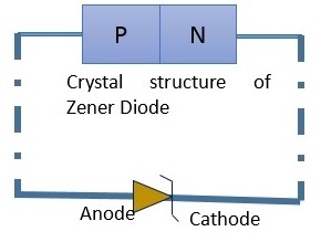
It is a specific type of semiconductor diode, which is made to operate in the reverse breakdown region. The following figure depicts the crystal structure and the symbol of a Zener diode. It is mostly similar to that of a conventional diode. However, small modification is done to distinguish it from a symbol of a regular diode. The bent line indicates letter Z of the Zener.
The most significant difference in Zener diodes and regular PN junction diodes is in the mode which they are used in circuits. These diodes are normally operated only in the reverse bias direction, which implies that the anode must be connected to the negative side of the voltage source and the cathode to the positive.
If a regular diode is used in the same way as Zener diode, it will be destroyed due to excessive current. This property makes the Zener diode less significant.
The following illustration shows a regulator with a Zener diode.
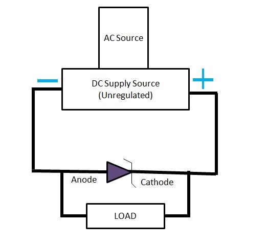
The Zener diode is connected in reverse bias direction across unregulated DC supply source. It is heavily doped so that the reverse breakdown voltage is reduced. This results in a very thin depletion layer. Due to this, the Zener diode has sharp reverse breakdown voltage Vz.
As per the circuit action, breakdown occurs sharply with a sudden increase in current as shown in the following figure.
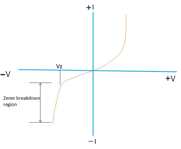
Voltage Vz remains constant with an increase in current. Due to this property, Zener diode is widely used in voltage regulation. It provides almost constant output voltage irrespective of the change in current through the Zener. Thus, the load voltage remains at a constant value.
We can see that at a particular reverse voltage known as knee voltage, current increases sharply with constant voltage. Due to this property, Zener diodes are widely used in voltage stabilization.
Semiconductor Devices - Photo Diode
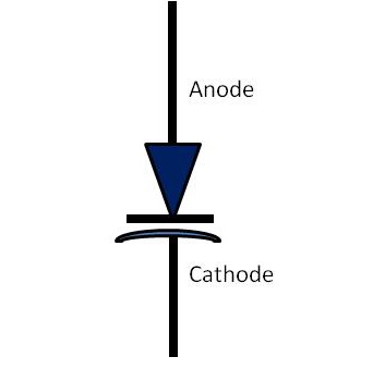
A photodiode is a P-N junction diode that will conduct current when exposed to light. This diode is actually designed to operate in the reverse bias mode. It means that larger the intensity of falling light, the greater will be the reverse bias current.
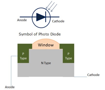
The following figure shows a schematic symbol and constructional detail of a photo diode.
Working of a Photo Diode
It is a reverse-biased diode. Reverse current increases as the intensity of incident light increases. This means that reverse current is directly proportional to the intensity of falling light.
It consists of a PN junction mounted on a P-type substrate and sealed in a metallic case. The junction point is made of transparent lens and it is the window where the light is supposed to fall.
As we know, when PN junction diode is reverse biased, a very small amount of reverse current flows. The reverse current is generated thermally by electron-hole pairs in the depletion region of the diode.
When light falls on PN junction, it is absorbed by the junction. This will generate more electron-hole pairs. Or we can say, characteristically, the amount of reverse current increases.
In other words, as the intensity of falling light increases, resistance of the PN junction diode decreases.
- This action makes the diode more conductive.
- These diodes have very fast response time
- These are used in high computing devices.
- It is also used in alarm circuits, counter circuits, etc.
Semiconductor Devices - Photovoltaic Cells
A basic photovoltaic cell consists of a n-type and a p-type semiconductor forming a p-n junction. The upper area is extended and transparent, generally exposed to the sun. These diodes or cells are exceptional that generate a voltage when exposed to light. The cells convert light energy directly into electrical energy.
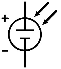
The following figure shows the symbol of photovoltaic cell.
Working of a Photovoltaic Cell
The construction of a photovoltaic cell is similar to that of a PN junction diode. There is no current flow through the device when no light is applied. In this state, the cell will not be able to generate current.
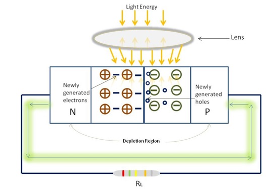
It is essential to bias the cell properly which requires a fair amount of light. As soon as light is applied, a remarkable state of PN junction diode can be observed. As a result, the electrons acquire sufficient energy and break away from the parent atoms. These newly generated electron-hole pairs in the depletion region crosses the junction.
In this action, the electrons move into the N type material because of its normal positive ion concentration. Likewise holes sweep into the P type material because of its negativeion content. This causes the N type material to instantly take on a negative charge and the P material to take on a positive charge. The P-N junction then delivers a small voltage as a response.
Characteristics of a Photovoltaic Cell
The following figure on the left, shows one of the characteristics, a graph between reverse current (IR) and illumination (E) of a photo diode. IR is measured on the vertical axis and illumination is measured on the horizontal axis. The graph is a straight line passing through the zero position.
i.e, IR = mE
m = graph straight line slope
The parameter m is the sensitivity of the diode.
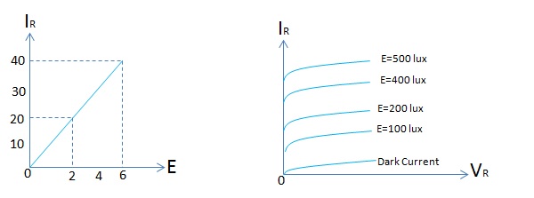
The figure on the right, shows another characteristic of the photo diode, a graph between reverse current (IR) and reverse voltage of a photo diode. It is clear from the graph that for a given reverse voltage, reverse current increases as the illumination increases on the PN junction.
These cells generally supply electrical power to a load device when light is applied. If a larger voltage is required, array of these cells are used to provide the same. For this reason, photovoltaic cells are used in applications where high levels of light energy are available.
Semiconductor Devices - Varactor Diode
This is a special P-N junction diode with an inconsistent concentration of impurities in its P-N materials. In a normal PN junction diode, doping impurities are usually dispersed equally throughout the material. Varactor diode doped with a very small quantity of impurities near the junction and impurity concentration increases moving away from the junction.
In conventional junction diode, the depletion region is an area which separates the P and N material. The depletion region is developed in the beginning when the junction is initially formed. There are no current carriers in this region and thus the depletion region acts as a dielectric medium or insulator.
The P-type material with holes as majority carriers and N type material with electrons as majority carriers now act as charged plates. Thus the diode can be considered as a capacitor with N- and P-type opposite charged plates and the depletion region acts as dielectric. As we know, P and N materials, being semiconductors, are separated by a a depletion region insulator.
Diodes which are designed to respond to the capacitance effect under reverse bias are called varactors, varicap diodes, or voltage-variable capacitors.
The following figure shows the symbol of Varactor diode.
Varactor diodes are normally operated in the reverse bias condition. When the reverse bias increases, the width of the depletion region also increases resulting in less capacitance. This means when reverse bias decreases, a corresponding increase in capacitance can be seen. Thus, diode capacitance varies inversely proportional to the bias voltage. Usually this is not linear. It is operated between zero and the reverse breakdown voltage.
The capacitance of Varactor diode is expressed as −
$$C_T = E\frac{A}{W_d}$$
CT = Total capacitance of the junction
E = Permittivity of the semiconductor material
A = Cross-sectional area of the junction
Wd = Width of the depletion layer
These diodes are variable used in microwave applications. Varactor diodes are also used in resonant circuits where some level of voltage tuning or frequency control is required. This diode is also employed in Automatic Frequency Control (AFC) in FM radio and television receivers.
Semiconductor Devices - Bipolar Transistors
Bipolar transistors are mainly formed of two layers of semiconductor material of the opposite type, connected back to back. The type of impurity added to silicon or germanium decides the polarity when it is formed.
NPN Transistor
An NPN transistor is composed of two N type material separated by a thin layer of P type semiconductor material. The crystal structure and schematic symbol of the NPN transistor are shown in the above figure.
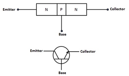
There are three leads taken out from each type of material recognized as the emitter, base, and collector. In the symbol, when the arrowhead of the emitter is directed outwards from the base, it indicates that the device is of the NPN type.
PNP Transistor
A PNP transistor is composed of two P type material separated by a thin layer of N type semiconductor material. The crystal structure and schematic symbol of a PNP transistor is shown below.
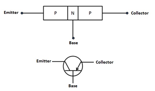
In the symbol, when the arrowhead of the emitter is directed inwards towards the base, it indicates that the device is of the PNP type.
Construction of a Transistor
Following are some manufacturing techniques used in the construction of a transistor −
Diffusion Type
In this method, the wafer of semiconductor is subjected to some gaseous diffusion of both N type and P type impurities to form emitter and collector junctions. First, base-collector junction is determined and photo-etched just prior to base diffusion. Later, the emitter is diffused on the base. Transistors manufactured by this technique have better noise figure and improvement in current gain is also seen.
Grown Type
It is formed by drawing a single crystal from melted silicon or germanium. The required concentration of impurity is added during crystal drawing operation.
Epitaxial Type
A very high purity and thin single-crystal layer of silicon or germanium is grown on a heavily doped substrate of the same type. This improved version of the crystal forms the collector on which the emitter and base junctions are formed.
Alloy Type
In this method, the base section is made of a thin slice of N type material. At the opposite sides of the slice, two small dots of Indium are attached and the complete formation is kept to a high temperature for a shorter time. The temperature would be above melting temperature of Indium and below Germanium. This technique is also known as fused construction.
Electrochemically Etched Type
In this method, on the opposite sides of a semiconductor wafer, depression is etched in order to reduce the width of the base region. Then a suitable metal is electroplated into the depressions area to form emitter and collector junctions.
Semiconductor Devices - Transistor Biasing
Transistors have three sections namely the emitter, the base, and the collector.
The base is much thinner than the emitter, and the collector is comparatively wider than both.
The emitter is heavily doped so that it can inject large number of charge carriers for current conduction.
The base passes most of the charge carriers to the collector as it is comparatively lightly doped than emitter and the collector.
For a proper functioning of the transistor, the emitter-base region must be forward-biased and collector-base region must be reverse-biased.
In semiconductor circuits, the source voltage is called as the bias voltage. In order to function, bipolar transistors must have both junctions biased. This condition causes a current to flow through the circuit. The depletion region of the device is reduced and majority current carriers are injected towards the junction. One of the junctions of a transistor must be forward biased and other must be reverse biased when it operates.
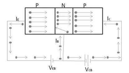
Working of NPN Transistor
As shown in the above figure, the emitter to base junction is forward biased and the collector to base junction is reverse biased. Forward bias on the emitter to base junction causes the electrons to flow from N type emitter towards the bias. This condition formulates the emitter current (IE).
While crossing the P-type material, electrons tend to combine with holes, generally very few, and constitute the base current (IB). Rest of the electrons cross the thin depletion region and reach the collector region. This current constitutes collector current (IC).
In other words, the emitter current actually flows through the collector circuit. Therefore, it can be considered that the emitter current is the summation of the base and the collector current. It can be expressed as,
IE = IB + IC
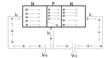
Working of PNP Transistor
As shown in the following figure, the emitter to base junction is forward biased and the collector to base junction is reverse biased. Forward bias on the emitter to base junction causes the holes to flow from P type emitter towards the bias. This condition formulates the emitter current (IE).
While crossing the N-type material, the electrons tend to combine with electrons, generally very few, and constitute the base current (IB). Rest of the holes cross the thin depletion region and reach the collector region. This current constitutes the collector current (IC).
In other words, the emitter current actually flows through the collector circuit. Therefore, it can be considered that the emitter current is the summation of the base and the collector current. It can be expressed as,
IE = IB + IC
Configuration of Transistors
When a transistor is connected in a circuit, four terminals or leads or legs are required, two both for input and output. As we know that transistors have only 3 terminals, this situation can be overcome by making one of the terminal common for both input and output section. Accordingly, a transistor can be connected in three configurations as follows −
- Common Base Configuration
- Common Emitter Configuration
- Common Collector Configuration
Following are some important points to note about transistor operation.
A transistor can be operated in three regions namely active, saturation, and cutoff region.
A transistor when used in the active region, the base-emitter junction is forward biased and the collector-base junction is reverse biased.
A transistor when used in the saturation region, the base-emitter junction is forward biased and the collector-base junction is also forward biased.
A transistor when used in the cut-off region, both the base-emitter junction and collector-base junction are reverse biased.
Comparison of Transistor Configuration
The following table shows the comparison of transistor configuration.
| Characteristics | Common Emitter | Common Base | Common Collector |
|---|---|---|---|
| Current Gain | High | No | Considerable |
| Applications | Audio frequency | High frequency | Impedance matching |
| Input Resistance | Low | Low | Very high |
| Output Resistance | High | Very high | Low |
| Voltage Gain | Approx. 500 | Approx. 150 | Less than 1 |
Advantages and Disadvantages of Transistors
The following table lists the advantages and disadvantages of transistors.
| Advantages | Disadvantages |
|---|---|
| Low source voltage | Temperature dependency |
| High voltage gain | Lower power dissipation |
| Smaller in size | Low input impedance |
Current Amplification Factor (α)
The ratio of change in the collector current to the change in the emitter current at constant collector to base voltage Vcb is known as current amplification factor α. It can be expressed as
$\alpha = \frac{\Delta I_C}{\Delta I_B}$ at Constant VCB
It is clear that current amplification factor is less than unity and it is inversely proportional to the base current considered that the base is lightly doped and thin.
Base Current Amplification Factor (β)
It is the ratio of change in collector current to the change in base current. A small variation in base current results in a very large change in collector current. Therefore, the transistor is able to attain current gain. It can be expressed as
$$\beta = \frac{\Delta I_C}{\Delta I_B}$$
Transistor as an Amplifier
The following figure shows that a load resistor (RL) is in series with the collector supply voltage (Vcc). A small voltage change ΔVi between the emitter and the base causes a relatively large emitter-current change ΔIE.
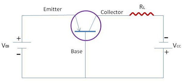
We define by the symbol a - the fraction of this current change - which is collected and passes through RL. The change in output voltage across the load resistor ΔVo = aRL ΔIE may be many times the change in input voltage ΔVI. Under these circumstances, the voltage amplification A == VO/ΔVI will be greater than unity and the transistor acts as an amplifier.
Field Effect Transistors
A Field Effect Transistor (FET) is a three-terminal semiconductor device. Its operation is based on a controlled input voltage. By appearance JFET and bipolar transistors are very similar. However, BJT is a current controlled device and JFET is controlled by input voltage. Most commonly two types of FETs are available.
- Junction Field Effect Transistor (JFET)
- Metal Oxide Semiconductor FET (IGFET)
Junction Field Effect Transistor
The functioning of Junction Field Effect Transistor depends upon the flow of majority carriers (electrons or holes) only. Basically, JFETs consist of an N type or P type silicon bar containing PN junctions at the sides. Following are some important points to remember about FET −
Gate − By using diffusion or alloying technique, both sides of N type bar are heavily doped to create PN junction. These doped regions are called gate (G).
Source − It is the entry point for majority carriers through which they enter into the semiconductor bar.
Drain − It is the exit point for majority carriers through which they leave the semiconductor bar.
Channel − It is the area of N type material through which majority carriers pass from the source to drain.
There are two types of JFETs commonly used in the field semiconductor devices: N-Channel JFET and P-Channel JFET.
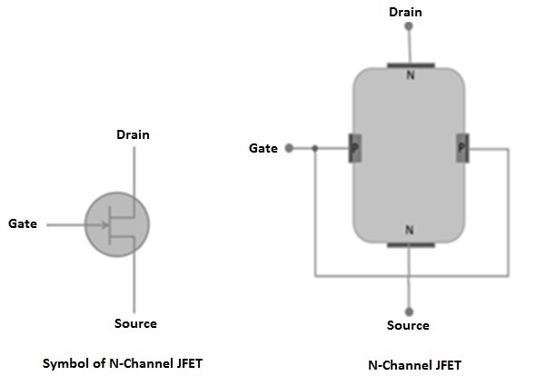
N-Channel JFET
It has a thin layer of N type material formed on P type substrate. Following figure shows the crystal structure and schematic symbol of an N-channel JFET. Then the gate is formed on top of the N channel with P type material. At the end of the channel and the gate, lead wires are attached and the substrate has no connection.
When a DC voltage source is connected to the source and the drain leads of a JFET, maximum current will flow through the channel. The same amount of current will flow from the source and the drain terminals. The amount of channel current flow will be determined by the value of VDD and the internal resistance of the channel.
A typical value of source-drain resistance of a JFET is quite a few hundred ohms. It is clear that even when the gate is open full current conduction will take place in the channel. Essentially, the amount of bias voltage applied at ID, controls the flow of current carriers passing through the channel of a JFET. With a small change in gate voltage, JFET can be controlled anywhere between full conduction and cutoff state.
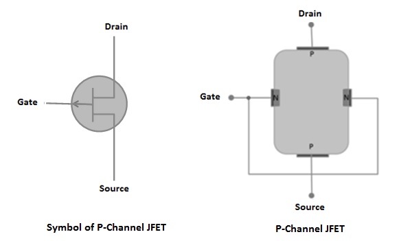
P-Channel JFETs
It has a thin layer of P type material formed on N type substrate. The following figure shows the crystal structure and schematic symbol of an N-channel JFET. The gate is formed on top of the P channel with N type material. At the end of the channel and the gate, lead wires are attached. Rest of the construction details are similar to that of N- channel JFET.
Normally for general operation, the gate terminal is made positive with respect to the source terminal. The size of the P-N junction depletion layer depends upon fluctuations in the values of reverse biased gate voltage. With a small change in gate voltage, JFET can be controlled anywhere between full conduction and cutoff state.
Output Characteristics of JFET
The output characteristics of JFET are drawn between drain current (ID) and drain source voltage (VDS) at constant gate source voltage (VGS) as shown in the following figure.
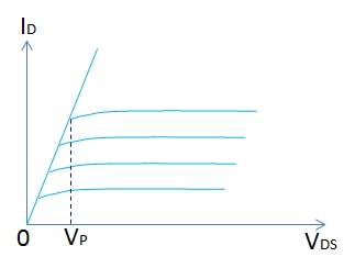
Initially, the drain current (ID) rises rapidly with drain source voltage (VDS) however suddenly becomes constant at a voltage known as pinch-off voltage (VP). Above pinch-off voltage, the channel width becomes so narrow that it allows very small drain current to pass through it. Therefore, drain current (ID) remains constant above pinch-off voltage.
Parameters of JFET
The main parameters of JFET are −
- AC drain resistance (Rd)
- Transconductance
- Amplification factor
AC drain resistance (Rd) − It is the ratio of change in the drain source voltage (ΔVDS) to the change in drain current (ΔID) at constant gate-source voltage. It can be expressed as,
Rd = (ΔVDS)/(ΔID) at Constant VGS
Transconductance (gfs) − It is the ratio of change in drain current (ΔID) to the change in gate source voltage (ΔVGS) at constant drain-source voltage. It can be expressed as,
gfs = (ΔID)/(ΔVGS) at constant VDS
Amplification Factor (u) − It is the ratio of change in drain-source voltage (ΔVDS) to the change in gate source voltage (ΔVGS) constant drain current (ΔID). It can be expressed as,
u = (ΔVDS)/(ΔVGS) at constant ID
Semiconductor Devices - JFET Biasing
There are two methods in use for biasing the JFET: Self-Bias Method and Potential Divider Method. In this chapter, we will discuss these two methods in detail.
Self-Bias Method
The following figure shows the self-bias method of n-channel JFET. The drain current flows through Rs and produces the required bias voltage. Therefore, Rs is the bias resistor.
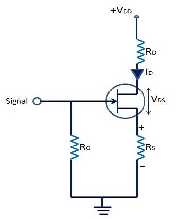
Therefore, voltage across bias resistor,
$$V_s = I_{DRS}$$
As we know, gate current is negligibly small, the gate terminal is at DC ground, VG = 0,
$$V_{GS} = V_G - V_s = 0 - I_{DRS}$$
Or $V_{GS} = -I_{DRS}$
VGS keeps gate negative w.r.t. to the source.
Voltage Divider Method
The following figure shows voltage divider method of biasing the JFETs. Here, resistor R1 and R2 form a voltage divider circuit across drain supply voltage (VDD), and it is more or less identical to the one used in transistor biasing.
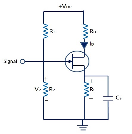
The voltage across R2 provides necessary bias −
$$V_2 = V_G = \frac{V_{DD}}{R_1 + R_2} \times R_2$$
$= V_2 + V_{GS} + I_D + R_S$
Or $V_{GS} = V_2 - I_{DRS}$
The circuit is so designed that VGS is always negative. The operating point can be found using the following formula −
$$I_D = \frac{V_2 - V_{GS}}{R_S}$$
and $V_{DS} = V_{DD} - I_D(R_D + R_S)$
Semiconductor Devices - MOSFET
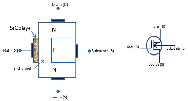
Metal-oxide semiconductor field-effect transistors, also known as MOSFETs, have greater importance and are a new addition to the FET family.
It has a lightly doped P type substrate into which two highly doped N type zones are diffused. A unique feature of this device is its gate construction. Here, the gate is completely insulated from the channel. When voltage is applied to the gate, it will develop an electrostatic charge.
At this point of time, no current is allowed to flow in the gate region of the device. Also, the gate is an area of the device, which is coated with metal. Generally, silicon dioxide is used as an insulating material between the gate and the channel. Due to this reason, it is also known as insulated gate FET. There are two MOSFETS widely used i) Depletion MOSFET ii) Enhancement MOSFET.
D MOSFET
The following figures show n-channel D-MOSFET and the symbol. The gate forms a capacitor with gate as one plate, and the other plate is the channel with SiO2 layer as dielectric. When the gate voltage varies, the electric field of the capacitor changes, which in turn varies the resistance of the n-channel.
In this case, we can either apply positive or negative voltage to the gate. When MOSFET is operated with negative gate voltage, it is called depletion mode and when operated with positive gate voltage it is called as enhancement mode of operation of MOSFET.
Depletion Mode
The following figure shows an n-channel D-MOSFET under depletion mode of operation.
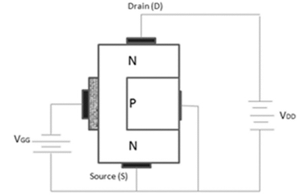
Its operation is as follows −
Most electrons are available on the gate as the gate is negative and it repels the electrons of n channel.
This action leaves positive ions in the part of the channel. In other words, some of the free electrons of the n channel are depleted. As a result, less number of electrons are available for current conduction through the n channel.
The greater the negative voltage at the gate, less is the current from the source to the drain. Thus, we can change the resistance of the n channel and the current from the source to the drain by varying the negative voltage on the gate.
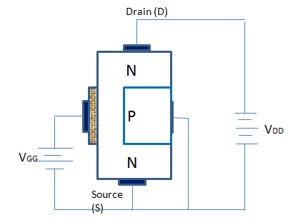
Enhancement Mode
The following figure shows n channel D MOSFET under enhancement mode of operation. Here, the gate acts as a capacitor. However, in this case the gate is positive. It provokes the electrons in the n channel and the number of electrons increases in the n channel.
A positive gate voltage enhances or increases conductivity of the channel. The larger the positive voltage on the gate, greater the conduction from the source to the drain.
Thus, we can change the resistance of the n channel and the current from the source to the drain by varying the positive voltage on the gate.
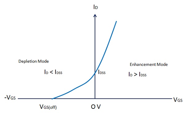
Transfer Characteristics of D MOSFET
The following figure shows transfer characteristics of D-MOSFET.
When VGS goes negative, ID falls below the value of IDSS, till it reaches zero and VGS = VGS (off) (Depletion mode). When VGS is zero, ID = IDSS because the gate and the source terminals are shorted. ID increases above the value of IDSS, when VGS is positive and the MOSFET is in enhancement mode.
Operational Amplifiers
An operational amplifier, or op-amp, is a very high gain differential amplifier with high input impedance and low output impedance. Operational amplifiers are typically used to provide voltage amplitude changes, oscillators, filter circuits, etc. An op-amp may contain a number of differential amplifier stages to achieve a very high voltage gain.
This is a high gain differential amplifier using direct coupling between the output and the input. This is suitable for DC as well as AC operations. Operational amplifiers perform numerous electronic functions such as instrumentation devices, signal generators, active filters, etc. besides various mathematical operations. This versatile device is also used in many nonlinear applications, such as voltage comparators, Analogtodigital converters and DigitaltoAnalog converters, Logarithmic amplifiers, nonlinear function generators, etc.
Basic Differential Amplifier
The following illustration shows a basic differential amplifier −
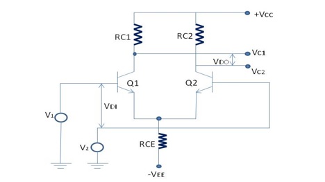
In the above figure −
VDI = differential input
VDI = V1 V2
VDO = differential output
VDO = VC1 - VC2
This amplifier amplifies the difference between the two input signals, V1 and V2.
Differential voltage gain,
$$A_d = \frac{V_{DO}}{V_{DI}}$$
and
$$A_d = \frac{(V_{C1} - V_{C2})}{V_{DI}}$$
As shown in the following figure, basic operational amplifier consists of three stages −
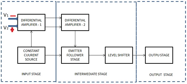
Input Stage
This is the first stage and has the following characteristics.
- High CMR (Common Mode Rejection)
- High input impedance
- Wide band width
- Low (DC) input offset
These are some significant characteristics for the performance of the operational amplifier. This stage consists of a differential amplifier stage and a transistor is biased so that it acts as a constant current source. The constant current source greatly increases the CMR of the differential amplifier.
Following are the two inputs to the differential amplifier −
- V1 = Non inverting input
- V2 = Inverting input
Intermediate Stage
This is the second stage and designed to get better voltage and current gains. The current gain is required to supply sufficient current to drive the output stage, where most of the operational amplifier power is generated. This stage consists of one or more differential amplifiers followed by an emitter follower and a DC level shifting stage. Level shifting circuit enables an amplifier to have two differential inputs with a single output.
| Vout = +ve | when V1 > V2 |
| Vout = -ve | when V2 < V1 |
| Vout = 0 | when V1 = V2 |
Output Stage
This is the last stage of the op-amp and is designed to have low output impedance. This provides the needed current to drive the load. More or less current will be drawn from the output stage as and when the load varies. Therefore, it is essential that the previous stage operates without being influenced by the output load. This requirement is met by designing this stage so as to have high input impedance and high current gain, however with low output impedance.
The operational amplifier has two inputs: Non-inverting input and Inverting input.
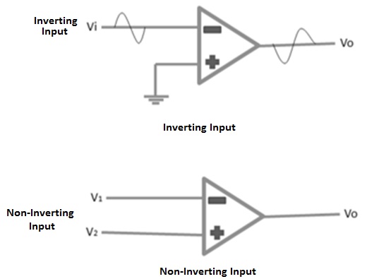
The above figure shows inverting type of operational amplifier. A signal which is applied at the inverting input terminal is amplified however the output signal is out of phase with the input signal by 180 degrees. A signal applied at the noninverting input terminal is amplified and the output signal is in phase with the input signal.
The op-amp can be connected in large number of circuits to provide various operating characteristics.
Semiconductor Devices - Practical Op-Amps
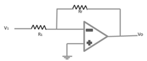
Inverting Amplifier
The following figure shows an inverting amplifier. The input signal is amplified and inverted. This is the most widely used constant-gain amplifier circuit.
Vo = -Rf.Vin /R1
Voltage gain A = (-Rf /R1)
Non-Inverting Amplifier
The following figure shows an op-amp circuit that works as a non-inverting amplifier or constant-gain multiplier and it has better frequency stability.
The input signal is amplified but it is not inverted.
Output Vo = [(R1 + Rf) / R1] V1
Voltage gain A = (R1 + Rf) / R1
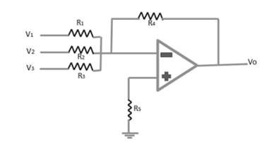
Inverting Summing Amplifier
The following figure shows an inverting summing amplifier. It is the most used circuit of the op-amp. The circuit shows a three-input summing amplifier, which provides a means of algebraically summing three voltages, each multiplied by a constant-gain factor. The output voltage is expressed as,
Vo = [(-R4 / R1) V1][(-R4 / R2) V2][(-R4 / R3) V3]
Vo = -R4(V1 / R1 + V2 / R2 + V3 / R3)
If, R1 = R2 = R3 = R4 = R & Rs = R/3
Vo = -(V1 + V2 + V3)
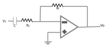
Semiconductor Devices - Integrator
The following figure shows that the feedback component used is a capacitor and the resulting connection is called as an integrator.
The virtual-ground equivalent shows that an expression for the voltage between the input and the output can be derived in terms of the current (I), from the input to the output. Recall that virtual ground means we can consider the voltage at the junction of R and XC to be ground (since Vi ≈ 0 V) however no current goes into the ground at that point. The capacitive impedance can be expressed as
$$X_C = \frac{1}{jwC} = \frac{1}{sC}$$
Where s = jw as in the Laplace notation. Solving equation for $V_o/V_i$ yields the following equation
$$I = \frac{V_1}{R_1} = \frac{-V_0}{X_c} = \frac{-\frac{V_0}{I}}{sC} = \frac{V_0}{V_1}$$
$$\frac{V_0}{V_1} = \frac{-1}{sCR_1}$$
It can be written in the time domain as
$$V_o(t) = -\frac{1}{RC}\int V_1(t)dt$$
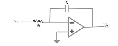
Semiconductor Devices - Differentiator
A differentiator circuit is shown in the following figure.
The differentiator provides a useful operation, the resulting relation for the circuit being
Vo(t) = RC(dv1(t)/dt
Following are some important parameters of Operational amplifier −
Open Loop Voltage Gain (AVOL)
The open loop voltage gain of an operational amplifier is its differential gain under conditions where no negative feedback is used. AVOL ranges from 74 db to 100 db.
AVOL = [Vo/(V1 V2)]
Output Offset Voltage (VOO)
The output offset voltage of an operational amplifier is its output voltage when its differential input voltage is zero.
Common Mode Rejection (CMR)
If both the inputs are at the same potential, causing the differential input zero, and if the output is zero, the operational amplifier is said to have a good common mode rejection.
Common Mode Gain (AC)
Common mode gain of an operational amplifier is the ratio of the common mode output voltage to the common mode input voltage.
Differential Gain (AD)
The differential gain of an operational amplifier is the ratio of the output to the differential input.
Ad = [Vo / (V1) - V2]
Common Mode Rejection Ratio (CMRR)
CMRR of an operational amplifier is defined as the ratio of the closed loop differential gain to the common mode gain.
CMRR = Ad/AC
Slew Rate (SR)
Slew rate is the rate of output voltage change caused by a step input voltage. An ideal slew rate is infinite, which means that the operational amplifier output should change instantly in response to an input step voltage.
We have already discussed some applications of op-amp such as differentiator, integrator, summing amplifier, etc. Some other common applications of operational amplifiers are −
- Logarithmic amplifier
- Gyrator (Inductance simulator)
- DC & AC voltage follower
- Analog to Digital converter
- Digital to Analog converter
- Power supplies for over voltage protection
- Polarity indicator
- Voltage follower
- Active filters
Semiconductor Devices - Oscillators
An oscillator is an electronic circuit that generates sinusoidal oscillations known as sinusoidal oscillator. It converts input energy from a DC source into AC output energy of periodic waveform, at a specific frequency and is known amplitude. The characteristic feature of the oscillator is that it maintains its AC output.
The following figure shows an amplifier with feedback signal even in the absence of an externally applied input signal. A sinusoidal oscillator is essentially a form of feedback amplifier, where special requirements are placed on the voltage gain Av and the feedback networks β.
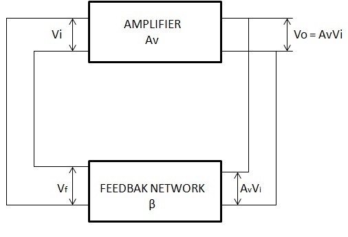
Consider the feedback amplifier of the above figure, where the feedback voltage Vf = βVO supplies the entire input voltage
$V_i = V_f = \beta V_0 = A_V\beta V_i$ (1)
$V_i = A_V\beta V_i$ Or $(1 - A_V\beta)V_i = 0$ (2)
If an output voltage is to be produced, the input voltage cannot be zero. Hence, for Vi to exist, Equation (2) requires that
$(1 - A_V\beta) = 0$ Or $A_V\beta = 1$ (3)
Equation (3) is known as Barkhausen criterion, which states two basic requirements for oscillation −
The voltage gain around the amplifier and feedback loop, called the loop gain, must be unity, or $A_V\beta = 1$.
The phase shift between $V_i$ and $V_f$, called the loop phase shift, must be zero.
If these two conditions are satisfied, the feedback amplifier of the above figure will generate a sinusoidal output waveform consistently.
Let us now discuss in detail about some typical oscillator circuits.
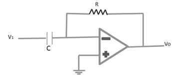
Phase Shift Oscillator
An oscillator circuit that follows the fundamental progress of a feedback circuit is the phase-shift oscillator. A phase-shift oscillator is shown in the following figure. The requirements for oscillation are that the loop gain (βA) should be greater than unity and the phase shift between input and output should be 360o.
Feedback is provided from the output of the RC network back to the amplifier input. The op-amp amplifier stage provides an initial 180-degree shift and the RC network introduces an additional amount of phase shift. At a specific frequency, the phase shift introduced by the network is exactly 180 degrees, so the loop will be 360 degrees and the feedback voltage is in phase input voltage.
The minimum number of RC stages in the feedback network is three, as each section provides 60 degrees of phase shift. The RC oscillator is ideally suited to the range of audio frequencies, from a few cycles to approximately 100 KHz. At the higher frequencies, the network impedance becomes so low that it may seriously load the amplifier, thereby reducing its voltage gain below the required minimum value, and the oscillations will cease.
At low frequencies, the loading effect is not usually a problem and the required large resistance and capacitance values are readily available. Using the basic network analysis, frequency oscillation can be expressed as
$$f = \frac{1}{2\pi RC \sqrt{6}}$$
Wien Bridge Oscillator
A practical oscillator circuit uses an op-amp and RC bridge circuit, with the oscillator frequency set by the R and C components. The following figure shows a basic version of a Wien bridge oscillator circuit.
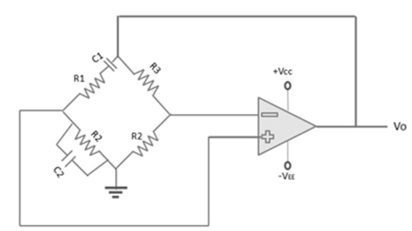
Note the basic bridge connection. Resistors R1 and R2 and capacitors C1 and C2 form the frequency-adjustment elements, while resistors R3 and R4 form part of the feedback path.
In this application, the input voltage (Vi) to the bridge is the amplifier output voltage, and the output voltage (Vo) of the bridge is feedback to the amplifier input. Neglecting the loading effects of the op-amp input and output impedances, the analysis of the bridge circuit results in
$$\frac{R_3}{R_4} = \frac{R_1}{R_2} + \frac{C_2}{C_1}$$
and
$$f = \frac{1}{2 \pi \sqrt{R_1C_1R_2C_2}}$$
If R1 = R2 = R and C1 = C2 = C, the resulting oscillator frequency is
$$f_o = \frac{1}{2\pi RC}$$
Hartley Oscillator
The following figure shows the Hartley oscillator. It is one of the most common RF circuits. It is normally used as the local oscillator in a communication broadcast receiver. The bipolar junction transistor in the common emitter connection is the voltage amplifier and is biased by a universal bias circuit consisting of R1, R2, RE. Emitter bypass capacitor (CE) increases the voltage gain of this single transistor stage.
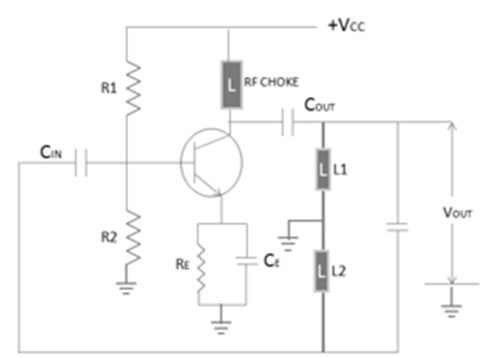
The Radio Frequency Choke (RFC) in the collector circuit acts as an open circuit at the RF frequency and prevents RF energy from entering the power supply. The tank circuit consists of L1, L2, and C. The frequency of oscillations is determined by the value of L1, L2, and C and is determined by the oscillates at the resonant frequency of the LC tank circuit. This resonant frequency is expressed as
$$f_o = \frac{1}{2\pi \sqrt{L_TC}}$$
The output signal can be taken from the collector by capacitive coupling, provided that the load is large and the frequency of oscillation is not affected.
Piezoelectricity
Piezoelectric properties are exhibited by a number of natural crystal substances, of which the most important are quartz, Rochelle salt, and tourmaline. When a sinusoidal voltage is applied across these materials, they vibrate at the applied voltage frequency.
On the other hand, when these materials are compressed and placed under mechanical strain to vibrate, they produce an equivalent sinusoidal voltage. Therefore, these materials are called as piezoelectric crystal. Quartz is the most popular piezoelectric crystal.
Crystal Oscillator
The circuit diagram of the crystal oscillator is shown in the following figure.
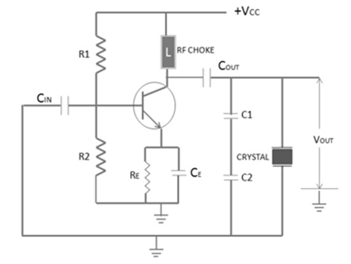
The crystal here acts as a tuned circuit. The equivalent circuit of a crystal is given below.
A crystal oscillator has two resonant frequencies: Series Resonant Frequency and Parallel Resonant Frequency.
Series Resonant Frequency
$$f_s = \frac{1}{2\pi \sqrt{LC}}$$
Parallel Resonant Frequency
$$f_p = \frac{1}{2\pi \sqrt{LC_T}}$$
The two resonant frequencies are almost same, since C/Cm is very small. In the above figure, the crystal is connected to operate in parallel resonant mode.
The resistors R1, R2, RE, and transistor together form an amplifier circuit. Resistors R1 and R2 provide a voltage stabilized DC bias. The capacitor (CE) provides AC bypass of the emitter resistor (RE) and the RFC provides high impedance to the frequency generated by the oscillator, so that they do not enter the power lines.
The crystal is in parallel with capacitor C1 and C2 and permits maximum voltage feedback from the collector to the emitter, when its impedance is maximum. At other frequencies, the crystal impedance is low and so the resultant feedback is too small to sustain oscillations. The oscillator frequency is stabilized at the parallel resonant frequency of the crystal.
Feedback & Compensation
The basic purpose of the bias network is to establish collectorbaseemitter voltage and current relationships at the operating point of the circuit (the operating point is also known as the quiescent point, Qpoint, nosignal point, idle point, or static point). Since, transistors rarely operate at this Q-point, the basic bias networks are generally used as a reference or starting point for design.
The actual circuit configuration and especially, the bias network values are selected on the basis of dynamic circuit conditions (desired output voltage swing, expected input signal level, etc.) Once the desired operating point is established, the next function of the bias network is to stabilize the amplifier circuit at this point. The basic bias network must maintain the desired current relationships in the presence of temperature and power supply changes, and possible transistor replacement.
In some cases, frequency changes and changes caused by the component again must also be offset by the bias network. This process is generally referred to as bias stabilization. Proper bias stabilization will maintain the amplifier circuit at the desired operating point (within practical limits), and will prevent thermal runaway.
Stability Factor S
It is defined as the rate of change of collector current w.r.t. reverse saturation current, keeping β and VBE constant. It is expressed as
$$S = \frac{\mathrm{d}I_c }{\mathrm{d} I_c}$$
Bias Stabilization Methods
The method of making the operating point independent of temperature changes or variations in transistors parameters is known as stabilization. There are several schemes for providing bias stabilization of solidstate amplifiers. All these schemes engage a form of negative feedback. That is any stage in transistor currents produce a corresponding voltage or current change that tends to counterbalance the initial change.
There are two fundamental methods for producing negative feedback, inversevoltage feedback and inversecurrent feedback.
Inverse-Voltage Feedback
The following figure shows the basic inversevoltage bias network. The emitterbase junction is forward biased by the voltage at the junction of R1 and R2. The basecollector junction is reverse biased by the differential between voltages at the collector and the base.
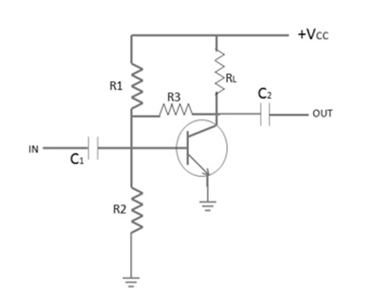
Normally, the collector of a resistance coupled amplifier is at a voltage about one half that of the supply Resistor (R3), connected between the collector and base. Since the collector voltage is positive, a portion of this voltage is feedback to the base to support the forward bias.
The normal (or Q point) forward bias on the emitterbase junction is the result of all the voltages between the emitter and the base. As the collector current increases, a larger voltage drop is produced across RL. As a result, the voltage on the collector decreases, reducing the voltage feedback to the base through R3. This reduces the emitterbase forward bias, reducing the emitter current and lowering the collector current to its normal value. As there is an initial decrease in the collector current, an opposite action takes place, and the collector current is raised to its normal (Q point) value.
Any form of negative or inverse feedback in an amplifier has a tendency to oppose all changes even those produced by the signal being amplified. This inverse or negative feedback tends to reduce and stabilize gain, as well as undesired change. This principle of stabilizing gain by means of feedback is used in more or less all types of amplifiers.
Inverse-Current Feedback
The following figure shows a distinctive inversecurrent (emitter feedback) bias network using an NPN transistor. Current feedback is more commonly used than voltage feedback in solidstate amplifiers. This is because transistors are mainly currentoperated devices, rather than voltageoperated devices.
The use of an emitterfeedback resistance in any bias circuit can be summed up as follows: Base current depends upon the differential in voltage between the base and the emitter. If the differential voltage is lowered, less base current will flow.
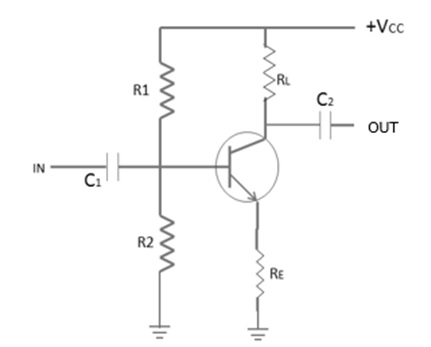
The opposite is true when the differential is increased. All current flowing through the collector. The voltage drops across the emitter resistor and is therefore not fully dependent. As the collector current increases, the emitter current and the voltage drop across the emitter resistor, will also increase. This negative feedback tends to decrease the differential between the base and the emitter, thus lowering the base current. In turn, the lower base current tends to decrease the collector current, and counterbalance the initial collectorcurrent increases.
Bias Compensation
In solid state amplifiers, when the loss in signal gain is intolerable in a particular application, compensating techniques are often used to reduce the drift of operating point. In order to provide maximum bias and thermal stabilization, both compensation and stabilization methods can be employed together.
The following figure shows diode compensation technique that utilized both the diode compensation and self-bias stabilization. If both diode and transistor are of the same type, then they have the same temperature coefficient across the circuit. Here, diode is forward biased. KVL for the given circuit can be expressed as −
$$I_c = \frac{\beta [V - (V_{BE} - V_o)] + (Rb + Rc)(\beta + 1)ICO}{Rb + Rc(1 + \beta)}$$
It is clear from the above equation that $V_{BE}$ follows VO w.r.t. temperature and Ic will have no effect to variations in $V_{BE}$. This is an effective method to take care of the operating point of the transistor due to variation in $V_{BE}$.
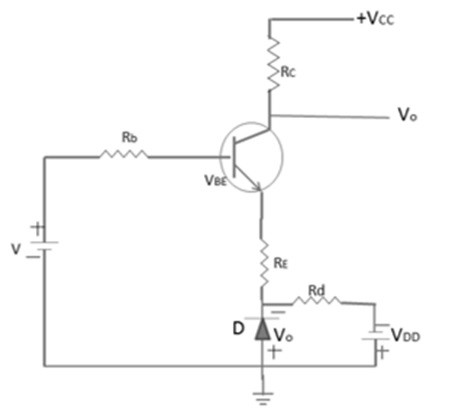
Temperature Compensation Device
We can also use some temperature sensitive device to compensate for variations of transistor internal characteristics. Thermistor has a negative temperature coefficient, which means with the rise in temperature, its resistance decreases exponentially. The following figure shows a circuit that uses thermistor (RT) to reduce the increase in collector current due to change in $V_{BE}$, ICO, or β with temperature.
When temperature increases, RT decreases and the current fed through RT into RE increases. The action voltage drop across RE is in the opposite direction to reverse bias the transistor. RT acts so as to tend to compensate the increase in IC, which increases due to the rise in temperature.
