
- Semiconductor Devices - Home
- Introduction
- Atomic Combinations
- Conduction in Solid Materials
- Conductivity & Mobility
- Types of Semiconductor
- Doping in Semiconductors
- Junction Diodes
- Depletion Zone
- Barrier Potential
- Junction Biasing
- Leakage Current
- Diode Characteristics
- Light Emitting Diode
- Zener Diode
- Photo Diode
- Photovoltaic Cells
- Varactor Diode
- Bipolar Transistors
- Construction of a Transistor
- Transistor Biasing
- Configuration of Transistors
- Field Effect Transistors
- JFET Biasing
- Semiconductor Devices - MOSFET
- Operational Amplifiers
- Practical Op-Amps
- Semiconductor Devices - Integrator
- Differentiator
- Oscillators
- Feedback & Compensation
- Semiconductor Devices - Quick Guide
- Semiconductor Devices - Resources
- Semiconductor Devices - Discussion
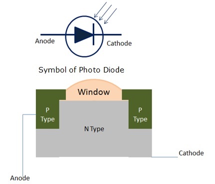
Semiconductor Devices - Photo Diode
A photodiode is a P-N junction diode that will conduct current when exposed to light. This diode is actually designed to operate in the reverse bias mode. It means that larger the intensity of falling light, the greater will be the reverse bias current.
The following figure shows a schematic symbol and constructional detail of a photo diode.
Working of a Photo Diode
It is a reverse-biased diode. Reverse current increases as the intensity of incident light increases. This means that reverse current is directly proportional to the intensity of falling light.
It consists of a PN junction mounted on a P-type substrate and sealed in a metallic case. The junction point is made of transparent lens and it is the window where the light is supposed to fall.
As we know, when PN junction diode is reverse biased, a very small amount of reverse current flows. The reverse current is generated thermally by electron-hole pairs in the depletion region of the diode.
When light falls on PN junction, it is absorbed by the junction. This will generate more electron-hole pairs. Or we can say, characteristically, the amount of reverse current increases.
In other words, as the intensity of falling light increases, resistance of the PN junction diode decreases.
- This action makes the diode more conductive.
- These diodes have very fast response time
- These are used in high computing devices.
- It is also used in alarm circuits, counter circuits, etc.
