
- Semiconductor Devices - Home
- Introduction
- Atomic Combinations
- Conduction in Solid Materials
- Conductivity & Mobility
- Types of Semiconductor
- Doping in Semiconductors
- Junction Diodes
- Depletion Zone
- Barrier Potential
- Junction Biasing
- Leakage Current
- Diode Characteristics
- Light Emitting Diode
- Zener Diode
- Photo Diode
- Photovoltaic Cells
- Varactor Diode
- Bipolar Transistors
- Construction of a Transistor
- Transistor Biasing
- Configuration of Transistors
- Field Effect Transistors
- JFET Biasing
- Semiconductor Devices - MOSFET
- Operational Amplifiers
- Practical Op-Amps
- Semiconductor Devices - Integrator
- Differentiator
- Oscillators
- Feedback & Compensation
- Semiconductor Devices - Quick Guide
- Semiconductor Devices - Resources
- Semiconductor Devices - Discussion
Semiconductor Devices - Leakage Current
An important conduction limitation of PN junction diode is leakage current. When a diode is reverse biased, the width of the depletion region increases. Generally, this condition is required to restrict the current carrier accumulation near the junction. Majority current carriers are primarily negated in the depletion region and hence the depletion region acts as an insulator. Normally, current carriers do not pass through an insulator.
It is seen that in a reverse-biased diode, some current flows through the depletion region. This current is called leakage current. Leakage current is dependent on minority current carriers. As we know that the minority carriers are electrons in the P type material and holes in the N type material.
The following figure shows how current carriers react when a diode is reverse biased.
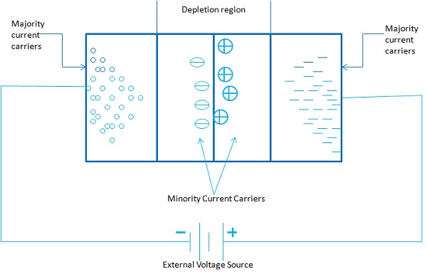
Following are the observations −
Minority carriers of each material are pushed through the depletion zone to the junction. This action causes a very small leakage current to occur. Generally, leakage current is so small that it can be considered as negligible.
Here, in case of leakage current, temperature plays an important role. The minority current carriers are mostly temperature dependent.
At room temperatures of 25C or 78F, there is negligible amount of minority carriers present in a reverse bias diode.
When the surrounding temperature rises, it causes significant increase in minority carrier creation and as a result it causes a corresponding increase in leakage current.
In all reverse-biased diodes, occurrence of leakage current is normal to some extent. In Germanium and Silicon diodes, leakage current is only of few microamperes and nanoamperes, respectively. Germanium is much more susceptible to temperature than silicon. For this reason, mostly Silicon is used in modern semiconductor devices.
