
- Semiconductor Devices - Home
- Introduction
- Atomic Combinations
- Conduction in Solid Materials
- Conductivity & Mobility
- Types of Semiconductor
- Doping in Semiconductors
- Junction Diodes
- Depletion Zone
- Barrier Potential
- Junction Biasing
- Leakage Current
- Diode Characteristics
- Light Emitting Diode
- Zener Diode
- Photo Diode
- Photovoltaic Cells
- Varactor Diode
- Bipolar Transistors
- Construction of a Transistor
- Transistor Biasing
- Configuration of Transistors
- Field Effect Transistors
- JFET Biasing
- Semiconductor Devices - MOSFET
- Operational Amplifiers
- Practical Op-Amps
- Semiconductor Devices - Integrator
- Differentiator
- Oscillators
- Feedback & Compensation
- Semiconductor Devices - Quick Guide
- Semiconductor Devices - Resources
- Semiconductor Devices - Discussion
Semiconductor Devices - JFET Biasing
There are two methods in use for biasing the JFET: Self-Bias Method and Potential Divider Method. In this chapter, we will discuss these two methods in detail.
Self-Bias Method
The following figure shows the self-bias method of n-channel JFET. The drain current flows through Rs and produces the required bias voltage. Therefore, Rs is the bias resistor.
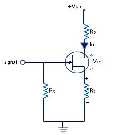
Therefore, voltage across bias resistor,
$$V_s = I_{DRS}$$
As we know, gate current is negligibly small, the gate terminal is at DC ground, VG = 0,
$$V_{GS} = V_G - V_s = 0 - I_{DRS}$$
Or $V_{GS} = -I_{DRS}$
VGS keeps gate negative w.r.t. to the source.
Voltage Divider Method
The following figure shows voltage divider method of biasing the JFETs. Here, resistor R1 and R2 form a voltage divider circuit across drain supply voltage (VDD), and it is more or less identical to the one used in transistor biasing.
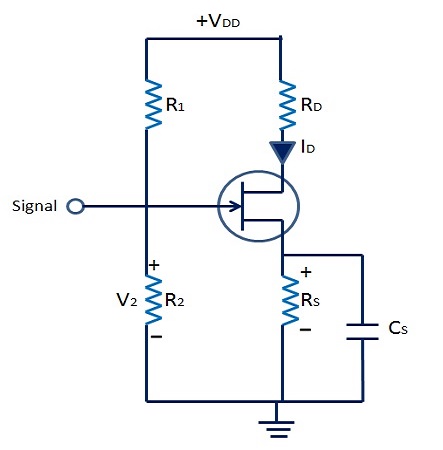
The voltage across R2 provides necessary bias −
$$V_2 = V_G = \frac{V_{DD}}{R_1 + R_2} \times R_2$$
$= V_2 + V_{GS} + I_D + R_S$
Or $V_{GS} = V_2 - I_{DRS}$
The circuit is so designed that VGS is always negative. The operating point can be found using the following formula −
$$I_D = \frac{V_2 - V_{GS}}{R_S}$$
and $V_{DS} = V_{DD} - I_D(R_D + R_S)$
