
- Semiconductor Devices - Home
- Introduction
- Atomic Combinations
- Conduction in Solid Materials
- Conductivity & Mobility
- Types of Semiconductor
- Doping in Semiconductors
- Junction Diodes
- Depletion Zone
- Barrier Potential
- Junction Biasing
- Leakage Current
- Diode Characteristics
- Light Emitting Diode
- Zener Diode
- Photo Diode
- Photovoltaic Cells
- Varactor Diode
- Bipolar Transistors
- Construction of a Transistor
- Transistor Biasing
- Configuration of Transistors
- Field Effect Transistors
- JFET Biasing
- Semiconductor Devices - MOSFET
- Operational Amplifiers
- Practical Op-Amps
- Semiconductor Devices - Integrator
- Differentiator
- Oscillators
- Feedback & Compensation
- Semiconductor Devices - Quick Guide
- Semiconductor Devices - Resources
- Semiconductor Devices - Discussion
Conduction in Solid Materials
The number of electrons in the outer ring of an atom is still the reason for the difference between conductors and insulators. As we know, solid materials are primarily used in electrical devices to accomplish electron conduction. These materials can be separated into conductors, semiconductors, and insulators.
However, conductors, semiconductors, and insulators are differentiated by energy-level diagrams. The amount of energy needed to cause an electron to leave its valence band and go into conduction will be accounted here. The diagram is a composite of all atoms within the material. Energy-level diagrams of insulators, semiconductors, and conductors are shown in the following figure.
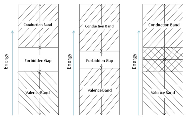
Valence Band
The bottom portion is the valence band. It represents the energy levels closest to the nucleus of the atom and the energy levels in the valance band hold the correct number of electron necessary to balance the positive charge of the nucleus. Thus, this band is called the filled band.
In the valence band, electrons are tightly bound to the nucleus. Moving upward in the energy level, the electrons are more lightly bound in each succeeding level toward the nucleus. It is not easy to disturb the electrons in the energy levels closer to the nucleus, as their movement requires larger energies and each electron orbit has a distinct energy level.
Conduction Band
The top or outermost band in the diagram is called the conduction band. If an electron has an energy level, which lies within this band, and is comparatively free to move around in the crystal, then it conducts electric current.
In semiconductor electronics, we are concerned mostly in the valence and conduction bands. Following are some basic information about it −
The valence band of each atom shows the energy levels of the valence electrons in the outer shell.
A definite amount of energy must be added to the valence electrons to cause them to go into the conduction band.
Forbidden Gap
The valence and conduction bands are separated by a gap, wherever exists, called forbidden gap. To cross the forbidden gap a definite amount of energy is needed. If it is insufficient, electrons are not released for conduction. Electrons will remain in the valence band till they receive additional energy to cross the forbidden gap.
The conduction status of a particular material can be indicated by the width of the forbidden gap. In atomic theory, the width of the gap is expressed in electron volts (eV). An electron volt is defined as the amount of energy gained or lost when an electron is subjected to a potential difference of 1 V. The atoms of each element have a dissimilar energy-level value that allows conduction.
Note that the forbidden region of an insulator is relatively wide. To cause an insulator to go into conduction will require a very large amount of energy. For example, Thyrite.
If insulators are operated at high temperatures, the increased heat energy causes the electrons of the valence band to move into the conduction band.
As it is clear from the energy band diagram, the forbidden gap of a semiconductor is much smaller than that of an insulator. For example, silicon needs to gain 0.7 eV of energy to go into the conduction band. At room temperature, the addition of heat energy may be sufficient to cause conduction in a semiconductor. This particular characteristic is of great importance in solid-state electronic devices.
In case of a conductor, the conduction band and the valence band partly overlaps one another. In a sense, there is no forbidden gap. Therefore, the electrons of valence band are able to release to become free electrons. Normally at normal room temperature little electrical conduction takes place within the conductor.
