
- Semiconductor Devices - Home
- Introduction
- Atomic Combinations
- Conduction in Solid Materials
- Conductivity & Mobility
- Types of Semiconductor
- Doping in Semiconductors
- Junction Diodes
- Depletion Zone
- Barrier Potential
- Junction Biasing
- Leakage Current
- Diode Characteristics
- Light Emitting Diode
- Zener Diode
- Photo Diode
- Photovoltaic Cells
- Varactor Diode
- Bipolar Transistors
- Construction of a Transistor
- Transistor Biasing
- Configuration of Transistors
- Field Effect Transistors
- JFET Biasing
- Semiconductor Devices - MOSFET
- Operational Amplifiers
- Practical Op-Amps
- Semiconductor Devices - Integrator
- Differentiator
- Oscillators
- Feedback & Compensation
- Semiconductor Devices - Quick Guide
- Semiconductor Devices - Resources
- Semiconductor Devices - Discussion
Field Effect Transistors
A Field Effect Transistor (FET) is a three-terminal semiconductor device. Its operation is based on a controlled input voltage. By appearance JFET and bipolar transistors are very similar. However, BJT is a current controlled device and JFET is controlled by input voltage. Most commonly two types of FETs are available.
- Junction Field Effect Transistor (JFET)
- Metal Oxide Semiconductor FET (IGFET)
Junction Field Effect Transistor
The functioning of Junction Field Effect Transistor depends upon the flow of majority carriers (electrons or holes) only. Basically, JFETs consist of an N type or P type silicon bar containing PN junctions at the sides. Following are some important points to remember about FET −
Gate − By using diffusion or alloying technique, both sides of N type bar are heavily doped to create PN junction. These doped regions are called gate (G).
Source − It is the entry point for majority carriers through which they enter into the semiconductor bar.
Drain − It is the exit point for majority carriers through which they leave the semiconductor bar.
Channel − It is the area of N type material through which majority carriers pass from the source to drain.
There are two types of JFETs commonly used in the field semiconductor devices: N-Channel JFET and P-Channel JFET.
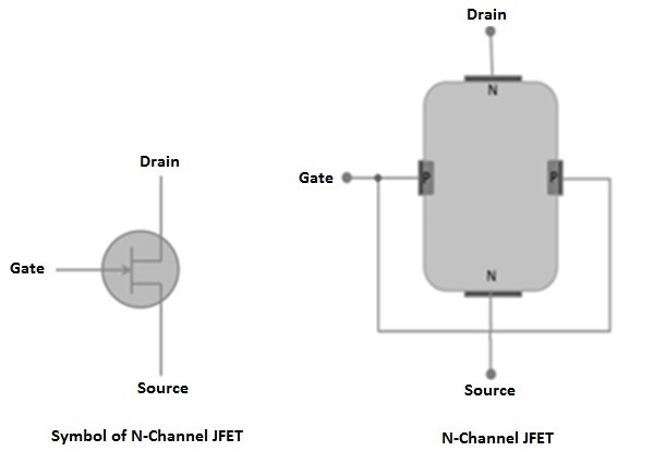
N-Channel JFET
It has a thin layer of N type material formed on P type substrate. Following figure shows the crystal structure and schematic symbol of an N-channel JFET. Then the gate is formed on top of the N channel with P type material. At the end of the channel and the gate, lead wires are attached and the substrate has no connection.
When a DC voltage source is connected to the source and the drain leads of a JFET, maximum current will flow through the channel. The same amount of current will flow from the source and the drain terminals. The amount of channel current flow will be determined by the value of VDD and the internal resistance of the channel.
A typical value of source-drain resistance of a JFET is quite a few hundred ohms. It is clear that even when the gate is open full current conduction will take place in the channel. Essentially, the amount of bias voltage applied at ID, controls the flow of current carriers passing through the channel of a JFET. With a small change in gate voltage, JFET can be controlled anywhere between full conduction and cutoff state.
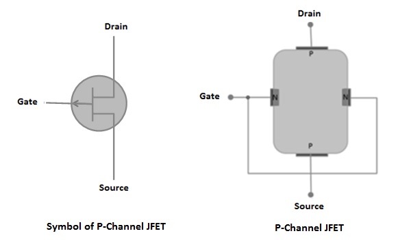
P-Channel JFETs
It has a thin layer of P type material formed on N type substrate. The following figure shows the crystal structure and schematic symbol of an N-channel JFET. The gate is formed on top of the P channel with N type material. At the end of the channel and the gate, lead wires are attached. Rest of the construction details are similar to that of N- channel JFET.
Normally for general operation, the gate terminal is made positive with respect to the source terminal. The size of the P-N junction depletion layer depends upon fluctuations in the values of reverse biased gate voltage. With a small change in gate voltage, JFET can be controlled anywhere between full conduction and cutoff state.
Output Characteristics of JFET
The output characteristics of JFET are drawn between drain current (ID) and drain source voltage (VDS) at constant gate source voltage (VGS) as shown in the following figure.
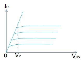
Initially, the drain current (ID) rises rapidly with drain source voltage (VDS) however suddenly becomes constant at a voltage known as pinch-off voltage (VP). Above pinch-off voltage, the channel width becomes so narrow that it allows very small drain current to pass through it. Therefore, drain current (ID) remains constant above pinch-off voltage.
Parameters of JFET
The main parameters of JFET are −
- AC drain resistance (Rd)
- Transconductance
- Amplification factor
AC drain resistance (Rd) − It is the ratio of change in the drain source voltage (ΔVDS) to the change in drain current (ΔID) at constant gate-source voltage. It can be expressed as,
Rd = (ΔVDS)/(ΔID) at Constant VGS
Transconductance (gfs) − It is the ratio of change in drain current (ΔID) to the change in gate source voltage (ΔVGS) at constant drain-source voltage. It can be expressed as,
gfs = (ΔID)/(ΔVGS) at constant VDS
Amplification Factor (u) − It is the ratio of change in drain-source voltage (ΔVDS) to the change in gate source voltage (ΔVGS) constant drain current (ΔID). It can be expressed as,
u = (ΔVDS)/(ΔVGS) at constant ID
