
- Semiconductor Devices - Home
- Introduction
- Atomic Combinations
- Conduction in Solid Materials
- Conductivity & Mobility
- Types of Semiconductor
- Doping in Semiconductors
- Junction Diodes
- Depletion Zone
- Barrier Potential
- Junction Biasing
- Leakage Current
- Diode Characteristics
- Light Emitting Diode
- Zener Diode
- Photo Diode
- Photovoltaic Cells
- Varactor Diode
- Bipolar Transistors
- Construction of a Transistor
- Transistor Biasing
- Configuration of Transistors
- Field Effect Transistors
- JFET Biasing
- Semiconductor Devices - MOSFET
- Operational Amplifiers
- Practical Op-Amps
- Semiconductor Devices - Integrator
- Differentiator
- Oscillators
- Feedback & Compensation
- Semiconductor Devices - Quick Guide
- Semiconductor Devices - Resources
- Semiconductor Devices - Discussion
Semiconductor Devices - Junction Biasing
The term bias refers to the application of DC voltage to set up certain operating conditions. Or when an external source of energy is applied to a P-N junction it is called a bias voltage or simply biasing. This method either increases or decreases the barrier potential of the junction. As a result, the reduction of the barrier potential causes current carriers to return to the depletion region. Following two bias conditions are applied w.r.t. PN junctions.
Forward Biasing − An external voltage is added of the same polarity to the barrier potential, which causes an increase in the width of the depletion region.
Reverse Biasing − A PN junction is biased in such a way that the application of external voltage action prevents current carriers from entering the depletion region.
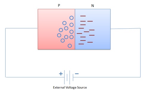
Forward Biasing
The following figure shows a forward biased PN junction diode with external voltage applied. You can see that the positive terminal of the battery is connected to the P material and the negative terminal of the battery is connected to the N material.
Following are the observations −
This bias voltage repels the majority current carriers of each P and N type material. As a result, large number of holes and electrons start appearing at the junction.
At the N-side of the junction, electrons move in to neutralize the positive ions in the depletion region.
On the P-side material, electrons are dragged from negative ions, which cause them to become neutral again. This means that forward biasing collapses the depletion region and hence the barrier potential too. It means that when P-N junction is forward biased, it will allow a continuous current flow.
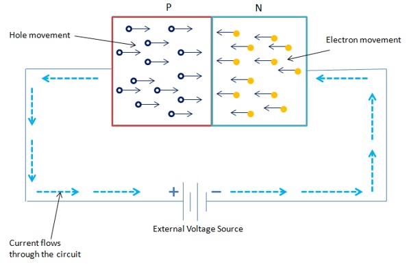
The following figure shows the flow of current carriers of a forward-biased diode. A constant supply of electrons is available due to an external voltage source connected to the diode. The flow and direction of the current is shown by large arrows outside the diode in the diagram. Note that the electron flow and the current flow refers to the same thing.
Following are the observations −
Suppose electrons flow through a wire from the negative battery terminal to the N material. Upon entering this material, they flow immediately to the junction.
Similarly, on the other side an equal number of electrons are pulled from P side and are returned to the positive battery terminal. This action creates new holes and causes them to move toward the junction.
When these holes and electrons reach the junction they join together and effectively disappear. As a result, new holes and electrons emerge at the outer ends of the diode. These majority carriers are created on a continuous basis. This action continues as long as the external voltage source is applied.
When diode is forward biased it can be noticed that electrons flow through the entire structure of diode. This is common in N type material, whereas in the P material holes are the moving current carriers. Notice that the hole movement in one direction must begin by electron movement in the opposite direction. Therefore, the total current flow is the addition of holes and electrons flow through a diode.
Reverse Biasing
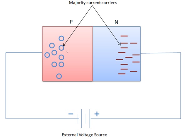
The following figure shows reverse biased PN junction diode with external voltage applied. You can see that the positive terminal of the battery is connected to the N material and the negative terminal of the battery is connected to the P material. Note that in such an arrangement, battery polarity is to oppose the material polarity of the diode so that dissimilar charges attract. Hence, majority charge carriers of each material are dragged away from the junction. Reverse biasing causes the diode to be nonconductive.
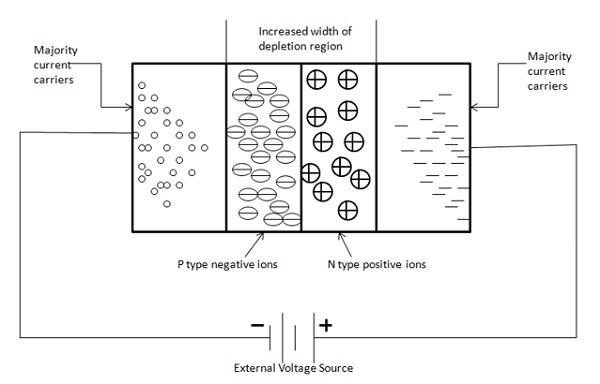
The following figure shows the arrangement of the majority current carriers in a reverse biased diode.
Following are the observations −
Due to circuit action electrons of the N material are pulled toward the positive battery terminal.
Each electron that moves or departs the diode causes a positive ion to emerge in its place. As a result, this causes an equivalent increase in the width of the depletion region on the N side of the junction.
The P side of the diode has a similar effect alike the N side. In this action, a number of electrons leave the negative battery terminal and enter the P type material.
These electrons then straight away move in and fill a number of holes. Each occupied hole then becomes a negative ion. These ions in turn are then repelled by the negative battery terminal and driven toward the junction. Due to this, there is an increase in the width of the depletion region on the P side of the junction.
The overall width of the depletion region directly depends on an external voltage source of a reverse-biased diode. In this case, the diode cannot efficiently support the current flow through the wide depletion region. As a result, the potential charge starts developing across the junction and increases until the barrier potential equals the external bias voltage. After this, the diode behaves as a nonconductor.
