
- Semiconductor Devices - Home
- Introduction
- Atomic Combinations
- Conduction in Solid Materials
- Conductivity & Mobility
- Types of Semiconductor
- Doping in Semiconductors
- Junction Diodes
- Depletion Zone
- Barrier Potential
- Junction Biasing
- Leakage Current
- Diode Characteristics
- Light Emitting Diode
- Zener Diode
- Photo Diode
- Photovoltaic Cells
- Varactor Diode
- Bipolar Transistors
- Construction of a Transistor
- Transistor Biasing
- Configuration of Transistors
- Field Effect Transistors
- JFET Biasing
- Semiconductor Devices - MOSFET
- Operational Amplifiers
- Practical Op-Amps
- Semiconductor Devices - Integrator
- Differentiator
- Oscillators
- Feedback & Compensation
- Semiconductor Devices - Quick Guide
- Semiconductor Devices - Resources
- Semiconductor Devices - Discussion
Feedback & Compensation
The basic purpose of the bias network is to establish collectorbaseemitter voltage and current relationships at the operating point of the circuit (the operating point is also known as the quiescent point, Qpoint, nosignal point, idle point, or static point). Since, transistors rarely operate at this Q-point, the basic bias networks are generally used as a reference or starting point for design.
The actual circuit configuration and especially, the bias network values are selected on the basis of dynamic circuit conditions (desired output voltage swing, expected input signal level, etc.) Once the desired operating point is established, the next function of the bias network is to stabilize the amplifier circuit at this point. The basic bias network must maintain the desired current relationships in the presence of temperature and power supply changes, and possible transistor replacement.
In some cases, frequency changes and changes caused by the component again must also be offset by the bias network. This process is generally referred to as bias stabilization. Proper bias stabilization will maintain the amplifier circuit at the desired operating point (within practical limits), and will prevent thermal runaway.
Stability Factor S
It is defined as the rate of change of collector current w.r.t. reverse saturation current, keeping β and VBE constant. It is expressed as
$$S = \frac{\mathrm{d}I_c }{\mathrm{d} I_c}$$
Bias Stabilization Methods
The method of making the operating point independent of temperature changes or variations in transistors parameters is known as stabilization. There are several schemes for providing bias stabilization of solidstate amplifiers. All these schemes engage a form of negative feedback. That is any stage in transistor currents produce a corresponding voltage or current change that tends to counterbalance the initial change.
There are two fundamental methods for producing negative feedback, inversevoltage feedback and inversecurrent feedback.
Inverse-Voltage Feedback
The following figure shows the basic inversevoltage bias network. The emitterbase junction is forward biased by the voltage at the junction of R1 and R2. The basecollector junction is reverse biased by the differential between voltages at the collector and the base.
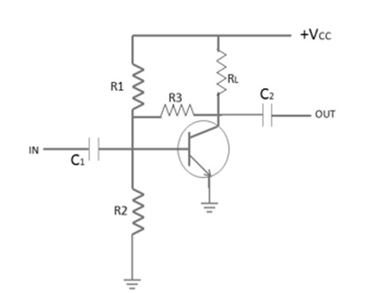
Normally, the collector of a resistance coupled amplifier is at a voltage about one half that of the supply Resistor (R3), connected between the collector and base. Since the collector voltage is positive, a portion of this voltage is feedback to the base to support the forward bias.
The normal (or Q point) forward bias on the emitterbase junction is the result of all the voltages between the emitter and the base. As the collector current increases, a larger voltage drop is produced across RL. As a result, the voltage on the collector decreases, reducing the voltage feedback to the base through R3. This reduces the emitterbase forward bias, reducing the emitter current and lowering the collector current to its normal value. As there is an initial decrease in the collector current, an opposite action takes place, and the collector current is raised to its normal (Q point) value.
Any form of negative or inverse feedback in an amplifier has a tendency to oppose all changes even those produced by the signal being amplified. This inverse or negative feedback tends to reduce and stabilize gain, as well as undesired change. This principle of stabilizing gain by means of feedback is used in more or less all types of amplifiers.
Inverse-Current Feedback
The following figure shows a distinctive inversecurrent (emitter feedback) bias network using an NPN transistor. Current feedback is more commonly used than voltage feedback in solidstate amplifiers. This is because transistors are mainly currentoperated devices, rather than voltageoperated devices.
The use of an emitterfeedback resistance in any bias circuit can be summed up as follows: Base current depends upon the differential in voltage between the base and the emitter. If the differential voltage is lowered, less base current will flow.
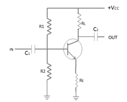
The opposite is true when the differential is increased. All current flowing through the collector. The voltage drops across the emitter resistor and is therefore not fully dependent. As the collector current increases, the emitter current and the voltage drop across the emitter resistor, will also increase. This negative feedback tends to decrease the differential between the base and the emitter, thus lowering the base current. In turn, the lower base current tends to decrease the collector current, and counterbalance the initial collectorcurrent increases.
Bias Compensation
In solid state amplifiers, when the loss in signal gain is intolerable in a particular application, compensating techniques are often used to reduce the drift of operating point. In order to provide maximum bias and thermal stabilization, both compensation and stabilization methods can be employed together.
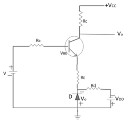
The following figure shows diode compensation technique that utilized both the diode compensation and self-bias stabilization. If both diode and transistor are of the same type, then they have the same temperature coefficient across the circuit. Here, diode is forward biased. KVL for the given circuit can be expressed as −
$$I_c = \frac{\beta [V - (V_{BE} - V_o)] + (Rb + Rc)(\beta + 1)ICO}{Rb + Rc(1 + \beta)}$$
It is clear from the above equation that $V_{BE}$ follows VO w.r.t. temperature and Ic will have no effect to variations in $V_{BE}$. This is an effective method to take care of the operating point of the transistor due to variation in $V_{BE}$.
Temperature Compensation Device
We can also use some temperature sensitive device to compensate for variations of transistor internal characteristics. Thermistor has a negative temperature coefficient, which means with the rise in temperature, its resistance decreases exponentially. The following figure shows a circuit that uses thermistor (RT) to reduce the increase in collector current due to change in $V_{BE}$, ICO, or β with temperature.
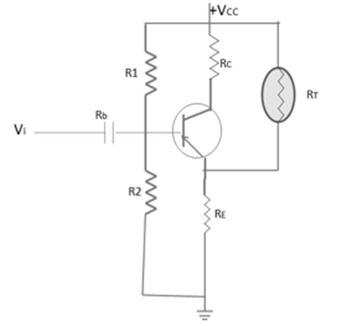
When temperature increases, RT decreases and the current fed through RT into RE increases. The action voltage drop across RE is in the opposite direction to reverse bias the transistor. RT acts so as to tend to compensate the increase in IC, which increases due to the rise in temperature.
