
- Semiconductor Devices - Home
- Introduction
- Atomic Combinations
- Conduction in Solid Materials
- Conductivity & Mobility
- Types of Semiconductor
- Doping in Semiconductors
- Junction Diodes
- Depletion Zone
- Barrier Potential
- Junction Biasing
- Leakage Current
- Diode Characteristics
- Light Emitting Diode
- Zener Diode
- Photo Diode
- Photovoltaic Cells
- Varactor Diode
- Bipolar Transistors
- Construction of a Transistor
- Transistor Biasing
- Configuration of Transistors
- Field Effect Transistors
- JFET Biasing
- Semiconductor Devices - MOSFET
- Operational Amplifiers
- Practical Op-Amps
- Semiconductor Devices - Integrator
- Differentiator
- Oscillators
- Feedback & Compensation
- Semiconductor Devices - Quick Guide
- Semiconductor Devices - Resources
- Semiconductor Devices - Discussion
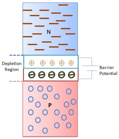
Semiconductor Devices - Barrier Potential
N-type and P-type material are considered as electrically neutral before they are joined together at a common junction. However, after joining diffusion takes place instantaneously, as electrons cross the junction to fill holes causing negative ions to emerge in the P material, this action causes the nearby area of the junction to take on a negative charge. Electrons departing the N material causes it to generate positive ions.
All this process, in turn, causes the N side of the junction to take on a net positive charge. This particular charge creation tends to force the remaining electrons and holes away from the junction. This action makes it somewhat hard for other charge carriers to diffuse across the junction. As a result, the charge is built up or barrier potential emerges across the junction.
As shown in the following figure. The resultant barrier potential has a small battery connected across the P-N junction. In the given figure observe the polarity of this potential barrier with respect to P and N material. This voltage or potential will exist when the crystal is not connected to an external source of energy.
The barrier potential of germanium is approximately 0.3 V, and of silicon is 0.7 V. These values cannot be measured directly and appears across the space charge region of the junction. In order to produce current conduction, the barrier potential of a P-N junction must be overcome by an external voltage source.
