
Article Categories
- All Categories
-
 Data Structure
-
 Networking
-
 RDBMS
RDBMS
-
 Operating System
-
 Java
Java
-
 MS Excel
-
 iOS
iOS
-
 HTML
HTML
-
 CSS
CSS
-
 Android
-
 Python
-
 C Programming
-
 C++
C++
-
 C#
C#
-
 MongoDB
-
 MySQL
MySQL
-
 Javascript
-
 PHP
PHP
-
 Economics & Finance
Selected Reading
Pins of 8259
Intel 8259 is designed as a 28-pin-programmable IC available as a package named DIP (Dual inline package). Its physical and functional pin diagrams are indicated below.
| PIN Name |
Description and Purposes |
|---|---|
| Vcc and Gnd |
It is the Power supply and ground pins. +5V power supply isused in this chip. |
| D7-0 |
For communication with the processor, there are Eight bi-directional data pins. |
| RD* |
It is active low-input pin activated by the processor to read the information status from the 8259. |
| WR* |
It is an active low-input pin which is activated by the processor to write the control information to 8259. |
| CS* |
For selecting the chip it is used an active low input pin. |
| A0 |
An address input pin used along with RD* and WR* which is used to identify the various command words. |
| IR0-IR7 |
There are Eight asynchronous interrupt request inputs. These interrupt requests can be programmed for level-trigger or edge-triggered mode. |
| INT |
A strong active high-output pin which interrupts the processor. Always connected to the INTR interrupt input of 8085. The INT output is only activated when all the given conditions are satisfied correctly. |
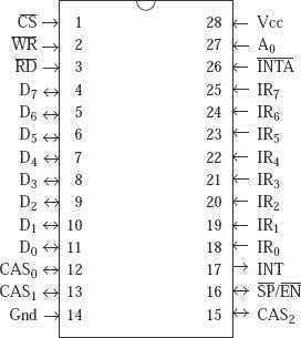
Fig − Pin diagram of Intel 8259
| INTA* |
It is termed as an active low-input pin. The 8259 receives the signal from INTA* to the output of 8085. 8085 sends the three consecutive INTA* signals, the 8259sends a 3-byte CALL instruction to the 8085 via D7-0 pins. The two bytes termed as second and third bytes of the CALL instruction contains the ISS address which depends on the IR input of 8259 that is going to be serviced. Fig: Functional pin diagram of 8259 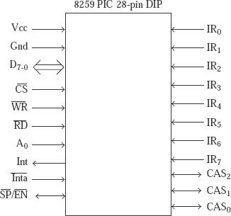
|
| CAS:2-0 |
These are cascaded lines. Used only when there are multiple 8259s in the system. The interrupt control system might have a master 8259 and maximum eight Slave 8259s. |
| SP*/EN* |
SP*/EN* stands for “slave program/enable buffer”. This pinserves dual function. When it is used as EN* pin it provides an active low-output pin that controls the buffer transceivers in the buffer mode. |

Updated on: 2020-06-29T05:52:04+05:30
7K+ Views

Advertisements