
Article Categories
- All Categories
-
 Data Structure
-
 Networking
-
 RDBMS
RDBMS
-
 Operating System
-
 Java
Java
-
 MS Excel
-
 iOS
iOS
-
 HTML
HTML
-
 CSS
CSS
-
 Android
-
 Python
-
 C Programming
-
 C++
C++
-
 C#
C#
-
 MongoDB
-
 MySQL
MySQL
-
 Javascript
-
 PHP
PHP
-
 Economics & Finance
Selected Reading
Pins of Z-80
The Zilog Z-80 is 40 pin DIP Microprocessor. Here we will see the actual pin level diagram of Z-80 and also the functional pin diagram of it.
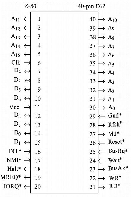
This is the actual pin diagram of Z-80 Microprocessor. Now we will see the functional pin diagram of it.
Now let us see the Pin functions of the Z-80 microprocessor.
| Pins | Type | Function |
|---|---|---|
| A15 – A0 |
Output |
16-bit address bus, which provides the addresses for memory (up to 64KB) |
| D7 – D0 |
Input/Output |
8-bit bi-directional data bus to transfer data between memory/IO devices and CPU. |
| BUSACK |
Output |
It is Bus Acknowledge pin. It indicates the requesting device that the address bus, data bus, control bus enter into a high impedance state. |
| BUSREQ |
Input |
Bus request Pin forces the address bus, data bus and control bus to enter a high impedance state. It is always recognized at the end of each machine cycle. |
| HALT | Output |
The Halt state indicates the CPU has executed a HALT instruction and waiting for interrupt. |
| INT | Input | Interrupt Request pin is used to generate interrupts by IO devices. After executing each instruction, CPU checks for the Interrupt requests |
| IORQ | Output |
The Input Output request pin is used to return low (0) signal when communication with IO ports is desired. |
| M1 | Output |
It indicates the Machine Cycle number 1. So the CPU activates this output, when the first machine cycle of an instruction is in progress. |
| MREQ | Output |
The memory request pin used to return low (0) signal, when communication with memory blocks is desired. |
| RD | Output |
It indicates that the CPU wants to read the data from memory or IO devices. |
| WR | Output |
It indicates the data bus contains to be stored at the addressed memory or IO locations. |
| NMI | Input |
The Non-Maskable Interrupt pin is negative edge triggered. Its priority is higher than the INT. It does not depend on the status of the interrupt enable flip-flops. It automatically forces the CPU to restart at location 0066H. |
| RESET | Input |
It resets the current interrupt enabled flip-flops, clears the Program Counter (PC), and the I and R registers. Address and data bus to a high impedance state. |
| RFSH | Output |
The RFSH and MREQ both can be used to indicate the lower seven bits of the address bus can be used as refresh address for Dynamic memories. |
| WAIT | Input |
This signal is used for the communication between CPU and memory units or IO devices. Until the signal is inactive the CPU continuously enters the Wait state. |
| CLK |
Input |
Single phase MOS level Clock |

Updated on: 2019-07-30T22:30:24+05:30
3K+ Views

Advertisements