- Microwave Engineering - Home
- Introduction
- Transmission Lines
- Modes of Propagation
- Types of Transmission Lines
- Waveguides
- Components
- Avalanche Transit Time Devices
- Microwave Devices
- E-Plane Tee
- H-Plane Tee
- E-H Plane Tee
- Rat-race Junction
- Directional Couplers
- Cavity Klystron
- Reflex Klystron
- Travelling Wave Tube
- Magnetrons
- Measurement Devices
- Measurements
- Example Problems
- Microwave Engineering -Quick Guide
- Microwave Engineering - Resources
- Microwave Engineering - Discussion
Microwave Engineering - Quick Guide
Microwave Engineering - Introduction
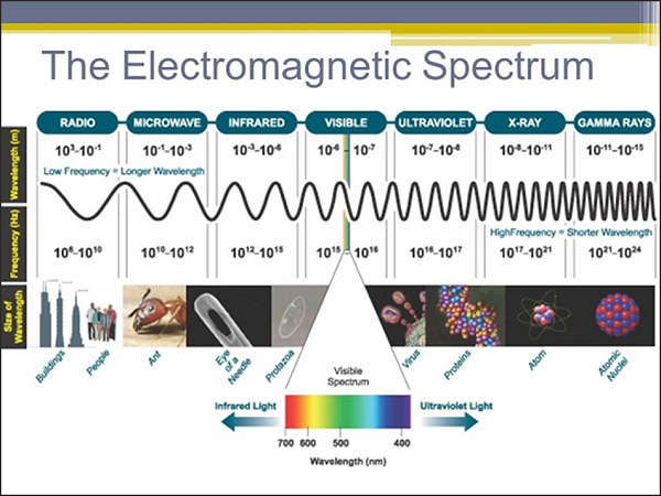
Electromagnetic Spectrum consists of entire range of electromagnetic radiation. Radiation is the energy that travels and spreads out as it propagates. The types of electromagnetic radiation that makes the electromagnetic spectrum is depicted in the following screenshot.
Let us now take a look at the properties of Microwaves.
Properties of Microwaves
Following are the main properties of Microwaves.
Microwaves are the waves that radiate electromagnetic energy with shorter wavelength.
Microwaves are not reflected by Ionosphere.
Microwaves travel in a straight line and are reflected by the conducting surfaces.
Microwaves are easily attenuated within shorter distances.
Microwave currents can flow through a thin layer of a cable.
Advantages of Microwaves
There are many advantages of Microwaves such as the following −
Supports larger bandwidth and hence more information is transmitted. For this reason, microwaves are used for point-to-point communications.
More antenna gain is possible.
Higher data rates are transmitted as the bandwidth is more.
Antenna size gets reduced, as the frequencies are higher.
Low power consumption as the signals are of higher frequencies.
Effect of fading gets reduced by using line of sight propagation.
Provides effective reflection area in the radar systems.
Satellite and terrestrial communications with high capacities are possible.
Low-cost miniature microwave components can be developed.
Effective spectrum usage with wide variety of applications in all available frequency ranges of operation.
Disadvantages of Microwaves
There are a few disadvantages of Microwaves such as the following −
- Cost of equipment or installation cost is high.
- They are hefty and occupy more space.
- Electromagnetic interference may occur.
- Variations in dielectric properties with temperatures may occur.
- Inherent inefficiency of electric power.
Applications of Microwaves
There are a wide variety of applications for Microwaves, which are not possible for other radiations. They are −
Wireless Communications
- For long distance telephone calls
- Bluetooth
- WIMAX operations
- Outdoor broadcasting transmissions
- Broadcast auxiliary services
- Remote pickup unit
- Studio/transmitter link
- Direct Broadcast Satellite (DBS)
- Personal Communication Systems (PCSs)
- Wireless Local Area Networks (WLANs)
- Cellular Video (CV) systems
- Automobile collision avoidance system
Electronics
- Fast jitter-free switches
- Phase shifters
- HF generation
- Tuning elements
- ECM/ECCM (Electronic Counter Measure) systems
- Spread spectrum systems
Commercial Uses
- Burglar alarms
- Garage door openers
- Police speed detectors
- Identification by non-contact methods
- Cell phones, pagers, wireless LANs
- Satellite television, XM radio
- Motion detectors
- Remote sensing
Navigation
- Global navigation satellite systems
- Global Positioning System (GPS)
Military and Radar
Radars to detect the range and speed of the target.
SONAR applications
Air traffic control
Weather forecasting
Navigation of ships
Minesweeping applications
Speed limit enforcement
Military uses microwave frequencies for communications and for the above mentioned applications.
Research Applications
- Atomic resonances
- Nuclear resonances
Radio Astronomy
- Mark cosmic microwave background radiation
- Detection of powerful waves in the universe
- Detection of many radiations in the universe and earths atmosphere
Food Industry
- Microwave ovens used for reheating and cooking
- Food processing applications
- Pre-heating applications
- Pre-cooking
- Roasting food grains/beans
- Drying potato chips
- Moisture levelling
- Absorbing water molecules
Industrial Uses
- Vulcanizing rubber
- Analytical chemistry applications
- Drying and reaction processes
- Processing ceramics
- Polymer matrix
- Surface modification
- Chemical vapor processing
- Powder processing
- Sterilizing pharmaceuticals
- Chemical synthesis
- Waste remediation
- Power transmission
- Tunnel boring
- Breaking rock/concrete
- Breaking up coal seams
- Curing of cement
- RF Lighting
- Fusion reactors
- Active denial systems
Semiconductor Processing Techniques
- Reactive ion etching
- Chemical vapor deposition
Spectroscopy
- Electron Paramagnetic Resonance (EPR or ESR) Spectroscopy
- To know about unpaired electrons in chemicals
- To know the free radicals in materials
- Electron chemistry
Medical Applications
- Monitoring heartbeat
- Lung water detection
- Tumor detection
- Regional hyperthermia
- Therapeutic applications
- Local heating
- Angioplasty
- Microwave tomography
- Microwave Acoustic imaging
For any wave to propagate, there is the need of a medium. The transmission lines, which are of different types, are used for the propagation of Microwaves. Let us learn about them in the next chapter.
Microwave Engineering - Transmission Lines
A transmission line is a connector which transmits energy from one point to another. The study of transmission line theory is helpful in the effective usage of power and equipment.
There are basically four types of transmission lines −
- Two-wire parallel transmission lines
- Coaxial lines
- Strip type substrate transmission lines
- Waveguides
While transmitting or while receiving, the energy transfer has to be done effectively, without the wastage of power. To achieve this, there are certain important parameters which has to be considered.
Main Parameters of a Transmission Line
The important parameters of a transmission line are resistance, inductance, capacitance and conductance.
Resistance and inductance together are called as transmission line impedance.
Capacitance and conductance together are called as admittance.
Resistance
The resistance offered by the material out of which the transmission lines are made, will be of considerable amount, especially for shorter lines. As the line current increases, the ohmic loss $\left ( I^{2}R \: loss \right )$ also increases.
The resistance $R$ of a conductor of length "$l$" and cross-section "$a$" is represented as
$$R = \rho \frac{l}{a}$$
Where
$\rho$ = resistivity of the conductor material, which is constant.
Temperature and the frequency of the current are the main factors that affect the resistance of a line. The resistance of a conductor varies linearly with the change in temperature. Whereas, if the frequency of the current increases, the current density towards the surface of the conductor also increases. Otherwise, the current density towards the center of the conductor increases.
This means, more the current flows towards the surface of the conductor, it flows less towards the center, which is known as the Skin Effect.
Inductance
In an AC transmission line, the current flows sinusoidally. This current induces a magnetic field perpendicular to the electric field, which also varies sinusoidally. This is well known as Faraday's law. The fields are depicted in the following figure.
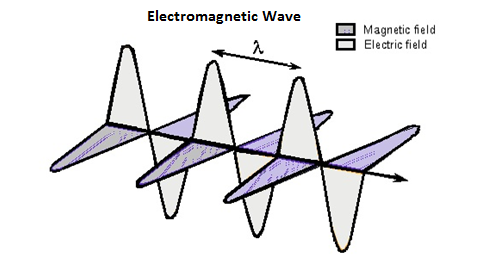
This varying magnetic field induces some EMF into the conductor. Now this induced voltage or EMF flows in the opposite direction to the current flowing initially. This EMF flowing in the opposite direction is equivalently shown by a parameter known as Inductance, which is the property to oppose the shift in the current.
It is denoted by "L". The unit of measurement is "Henry(H)".
Conductance
There will be a leakage current between the transmission line and the ground, and also between the phase conductors. This small amount of leakage current generally flows through the surface of the insulator. Inverse of this leakage current is termed as Conductance. It is denoted by "G".
The flow of line current is associated with inductance and the voltage difference between the two points is associated with capacitance. Inductance is associated with the magnetic field, while capacitance is associated with the electric field.
Capacitance
The voltage difference between the Phase conductors gives rise to an electric field between the conductors. The two conductors are just like parallel plates and the air in between them becomes dielectric. This pattern gives rise to the capacitance effect between the conductors.
Characteristic Impedance
If a uniform lossless transmission line is considered, for a wave travelling in one direction, the ratio of the amplitudes of voltage and current along that line, which has no reflections, is called as Characteristic impedance.
It is denoted by $Z_0$
$$Z_0 = \sqrt{\frac{voltage \:\: wave \:\: value}{current \:\: wave \:\: value}}$$
$$Z_0 = \sqrt{\frac{R + jwL}{G + jwC}}$$
For a lossless line, $R_0 = \sqrt{\frac{L}{C}}$
Where $L$ & $C$ are the inductance and capacitance per unit lengths.
Impedance Matching
To achieve maximum power transfer to the load, impedance matching has to be done. To achieve this impedance matching, the following conditions are to be met.
The resistance of the load should be equal to that of the source.
$$R_L = R_S$$
The reactance of the load should be equal to that of the source but opposite in sign.
$$X_L = -X_S$$
Which means, if the source is inductive, the load should be capacitive and vice versa.
Reflection Co-efficient
The parameter that expresses the amount of reflected energy due to impedance mismatch in a transmission line is called as Reflection coefficient. It is indicated by $\rho$ (rho).
It can be defined as "the ratio of reflected voltage to the incident voltage at the load terminals".
$$\rho = \frac{reflected\:voltage}{incident\:voltage} = \frac{V_r}{V_i} \: at \: load \: terminals$$
If the impedance between the device and the transmission line don't match with each other, then the energy gets reflected. The higher the energy gets reflected, the greater will be the value of $\rho$ reflection coefficient.
Voltage Standing Wave Ratio (VSWR)
The standing wave is formed when the incident wave gets reflected. The standing wave which is formed, contains some voltage. The magnitude of standing waves can be measured in terms of standing wave ratios.
The ratio of maximum voltage to the minimum voltage in a standing wave can be defined as Voltage Standing Wave Ratio (VSWR). It is denoted by "$S$".
$$S = \frac{\left |V_{max} \right |}{\left |V_{min} \right |} \quad 1\:\leq S \leq \infty$$
VSWR describes the voltage standing wave pattern that is present in the transmission line due to phase addition and subtraction of the incident and reflected waves.
Hence, it can also be written as
$$S = \frac{1 + \rho }{1 - \rho }$$
The larger the impedance mismatch, the higher will be the amplitude of the standing wave. Therefore, if the impedance is matched perfectly,
$$V_{max} : V_{min} = 1:1$$
Hence, the value for VSWR is unity, which means the transmission is perfect.
Efficiency of Transmission Lines
The efficiency of transmission lines is defined as the ratio of the output power to the input power.
$\% \: efficiency \: of \: transmission \: line \: \eta = \frac{Power \: delivered \: at \: reception}{Power \: sent \: from \: the \: transmission \: end} \times 100$
Voltage Regulation
Voltage regulation is defined as the change in the magnitude of the voltage between the sending and receiving ends of the transmission line.
$\% \: voltage \: regulation = \frac{sending \: end \: voltage - \: receiving \: end \: voltage}{sending \: end \: voltage} \times 100$
Losses due to Impedance Mismatch
The transmission line, if not terminated with a matched load, occurs in losses. These losses are many types such as attenuation loss, reflection loss, transmission loss, return loss, insertion loss, etc.
Attenuation Loss
The loss that occurs due to the absorption of the signal in the transmission line is termed as Attenuation loss, which is represented as
$$Attenuation \: loss (dB) = 10 \: log_{10} \left [ \frac{E_i - E_r}{E_t} \right ]$$
Where
$E_i$ = the input energy
$E_r$ = the reflected energy from the load to the input
$E_t$ = the transmitted energy to the load
Reflection Loss
The loss that occurs due to the reflection of the signal due to impedance mismatch of the transmission line is termed as Reflection loss, which is represented as
$$Reflection \: loss (dB) = 10 \: log_{10} \left [ \frac{E_i}{E_i - E_r} \right ]$$
Where
$E_i$ = the input energy
$E_r$ = the reflected energy from the load
Transmission Loss
The loss that occurs while transmission through the transmission line is termed as Transmission loss, which is represented as
$$Transmission \: loss(dB) = 10 \: log_{10} \: \frac{E_i}{E_t}$$
Where
$E_i$ = the input energy
$E_t$ = the transmitted energy
Return Loss
The measure of the power reflected by the transmission line is termed as Return loss, which is represented as
$$Return \: loss(dB) = 10 \: log_{10} \: \frac{E_i}{E_r}$$
Where
$E_i$ = the input energy
$E_r$ = the reflected energy
Insertion Loss
The loss that occurs due to the energy transfer using a transmission line compared to energy transfer without a transmission line is termed as Insertion loss, which is represented as
$$Insertion \: loss(dB) = 10 \: log_{10} \: \frac{E_1}{E_2}$$
Where
$E_1$ = the energy received by the load when directly connected to the source, without a transmission line.
$E_2$ = the energy received by the load when the transmission line is connected between the load and the source.
Stub Matching
If the load impedance mismatches the source impedance, a method called "Stub Matching" is sometimes used to achieve matching.
The process of connecting the sections of open or short circuit lines called stubs in the shunt with the main line at some point or points, can be termed as Stub Matching.
At higher microwave frequencies, basically two stub matching techniques are employed.
Single Stub Matching
In Single stub matching, a stub of certain fixed length is placed at some distance from the load. It is used only for a fixed frequency, because for any change in frequency, the location of the stub has to be changed, which is not done. This method is not suitable for coaxial lines.
Double Stub Matching
In double stud matching, two stubs of variable length are fixed at certain positions. As the load changes, only the lengths of the stubs are adjusted to achieve matching. This is widely used in laboratory practice as a single frequency matching device.
The following figures show how the stub matchings look.
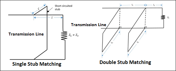
The single stub matching and double stub matching, as shown in the above figures, are done in the transmission lines to achieve impedance matching.
Modes of Propagation
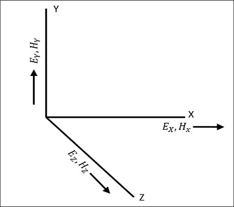
A wave has both electric and magnetic fields. All transverse components of electric and magnetic fields are determined from the axial components of electric and magnetic field, in the z direction. This allows mode formations, such as TE, TM, TEM and Hybrid in microwaves. Let us have a look at the types of modes.
The direction of the electric and the magnetic field components along three mutually perpendicular directions x, y, and z are as shown in the following figure.
Types of Modes
The modes of propagation of microwaves are −
TEM (Transverse Electromagnetic Wave)
In this mode, both the electric and magnetic fields are purely transverse to the direction of propagation. There are no components in $'Z'$ direction.
$$E_z = 0 \: and \: H_z = 0$$
TE (Transverse Electric Wave)
In this mode, the electric field is purely transverse to the direction of propagation, whereas the magnetic field is not.
$$E_z = 0 \: and \: H_z \ne 0$$
TM (Transverse Magnetic Wave)
In this mode, the magnetic field is purely transverse to the direction of propagation, whereas the electric field is not.
$$E_z \ne 0 \: and \: H_z = 0$$
HE (Hybrid Wave)
In this mode, neither the electric nor the magnetic field is purely transverse to the direction of propagation.
$$E_z \ne 0 \: and \: H_z \ne 0$$
Multi conductor lines normally support TEM mode of propagation, as the theory of transmission lines is applicable to only those system of conductors that have a go and return path, i.e., those which can support a TEM wave.
Waveguides are single conductor lines that allow TE and TM modes but not TEM mode. Open conductor guides support Hybrid waves. The types of transmission lines are discussed in the next chapter.
Types of Transmission Lines
The conventional open-wire transmission lines are not suitable for microwave transmission, as the radiation losses would be high. At Microwave frequencies, the transmission lines employed can be broadly classified into three types. They are −
- Multi conductor lines
- Co-axial lines
- Strip lines
- Micro strip lines
- Slot lines
- Coplanar lines, etc.
- Single conductor lines (Waveguides)
- Rectangular waveguides
- Circular waveguides
- Elliptical waveguides
- Single-ridged waveguides
- Double-ridged waveguides, etc.
- Open boundary structures
- Di-electric rods
- Open waveguides, etc.
Multi-conductor Lines
The transmission lines which has more than one conductor are called as Multi-conductor lines.
Co-axial Lines
This one is mostly used for high frequency applications.
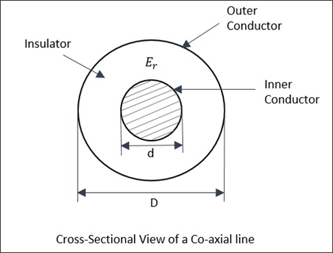
A coaxial line consists of an inner conductor with inner diameter d, and then a concentric cylindrical insulating material, around it. This is surrounded by an outer conductor, which is a concentric cylinder with an inner diameter D. This structure is well understood by taking a look at the following figure.
The fundamental and dominant mode in co-axial cables is TEM mode. There is no cutoff frequency in the co-axial cable. It passes all frequencies. However, for higher frequencies, some higher order non-TEM mode starts propagating, causing a lot of attenuation.
Strip Lines
These are the planar transmission lines, used at frequencies from 100MHz to 100GHz.
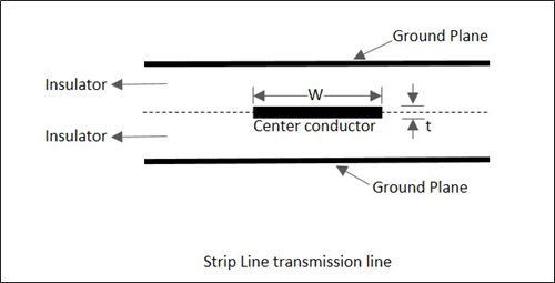
A Strip line consists of a central thin conducting strip of width ω which is greater than its thickness t. It is placed inside the low loss dielectric (εr) substrate of thickness b/2 between two wide ground plates. The width of the ground plates is five times greater than the spacing between the plates.
The thickness of metallic central conductor and the thickness of metallic ground planes are the same. The following figure shows the cross-sectional view of the strip line structure.
The fundamental and dominant mode in Strip lines is TEM mode. For b<λ/2, there will be no propagation in the transverse direction. The impedance of a strip line is inversely proportional to the ratio of the width ω of the inner conductor to the distance b between the ground planes.
Micro Strip Lines
The strip line has a disadvantage that it is not accessible for adjustment and tuning. This is avoided in micro strip lines, which allows mounting of active or passive devices, and also allows making minor adjustments after the circuit has been fabricated.
A micro strip line is an unsymmetrical parallel plate transmission line, having di-electric substrate which has a metallized ground on the bottom and a thin conducting strip on top with thickness 't' and width 'ω'. This can be understood by taking a look at the following figure, which shows a micro strip line.
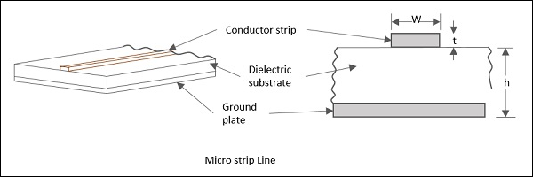
The characteristic impedance of a micro strip is a function of the strip line width (ω), thickness (t) and the distance between the line and the ground plane (h). Micro strip lines are of many types such as embedded micro strip, inverted micro strip, suspended micro strip and slotted micro strip transmission lines.
In addition to these, some other TEM lines such as parallel strip lines and coplanar strip lines also have been used for microwave integrated circuits.
Other Lines
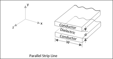
A Parallel Strip line is similar to a two conductor transmission line. It can support quasi TEM mode. The following figure explains this.
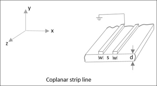
A Coplanar strip line is formed by two conducting strips with one strip grounded, both being placed on the same substrate surface, for convenient connections. The following figure explains this.
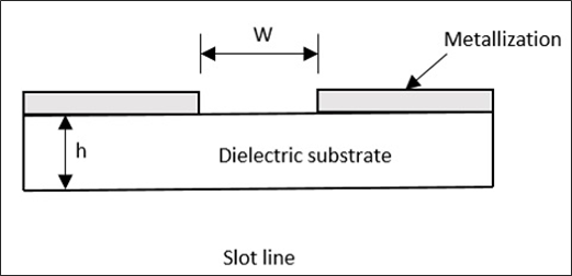
A Slot line transmission line, consists of a slot or gap in a conducting coating on a dielectric substrate and this fabrication process is identical to the micro strip lines. Following is its diagrammatical representation.
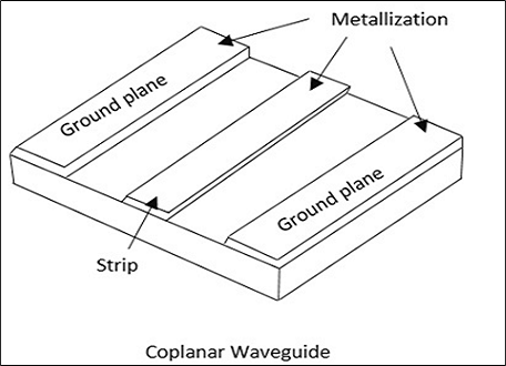
A coplanar waveguide consists of a strip of thin metallic film which is deposited on the surface of a dielectric slab. This slab has two electrodes running adjacent and parallel to the strip on to the same surface. The following figure explains this.
All of these micro strip lines are used in microwave applications where the use of bulky and expensive to manufacture transmission lines will be a disadvantage.
Open Boundary Structures
These can also be stated as Open Electromagnetic Waveguides. A waveguide that is not entirely enclosed in a metal shielding, can be considered as an open waveguide. Free space is also considered as a kind of open waveguide.
An open waveguide may be defined as any physical device with longitudinal axial symmetry and unbounded cross-section, capable of guiding electromagnetic waves. They possess a spectrum which is no longer discrete. Micro strip lines and optical fibers are also examples of open waveguides.
Microwave Engineering - Waveguides
Generally, if the frequency of a signal or a particular band of signals is high, the bandwidth utilization is high as the signal provides more space for other signals to get accumulated. However, high frequency signals can't travel longer distances without getting attenuated. We have studied that transmission lines help the signals to travel longer distances.
Microwaves propagate through microwave circuits, components and devices, which act as a part of Microwave transmission lines, broadly called as Waveguides.
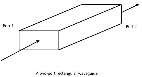
A hollow metallic tube of uniform cross-section for transmitting electromagnetic waves by successive reflections from the inner walls of the tube is called as a Waveguide.
The following figure shows an example of a waveguide.
A waveguide is generally preferred in microwave communications. Waveguide is a special form of transmission line, which is a hollow metal tube. Unlike a transmission line, a waveguide has no center conductor.
The main characteristics of a Waveguide are −
The tube wall provides distributed inductance.
The empty space between the tube walls provide distributed capacitance.
These are bulky and expensive.
Advantages of Waveguides
Following are few advantages of Waveguides.
Waveguides are easy to manufacture.
They can handle very large power (in kilo watts).
Power loss is very negligible in waveguides.
They offer very low loss (low value of alpha-attenuation).
When microwave energy travels through waveguide, it experiences lower losses than a coaxial cable.
Types of Waveguides
There are five types of waveguides.
- Rectangular waveguide
- Circular waveguide
- Elliptical waveguide
- Single-ridged waveguide
- Double-ridged waveguide
The following figures show the types of waveguides.
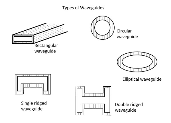
The types of waveguides shown above are hollow in the center and made up of copper walls. These have a thin lining of Au or Ag on the inner surface.
Let us now compare the transmission lines and waveguides.
Transmission Lines Vs Waveguides
The main difference between a transmission line and a wave guide is −
A two conductor structure that can support a TEM wave is a transmission line.
A one conductor structure that can support a TE wave or a TM wave but not a TEM wave is called as a waveguide.
The following table brings out the differences between transmission lines and waveguides.
| Transmission Lines | Waveguides |
|---|---|
| Supports TEM wave | Cannot support TEM wave |
| All frequencies can pass through | Only the frequencies that are greater than cut-off frequency can pass through |
| Two conductor transmission | One conductor transmission |
| Reflections are less | A wave travels through reflections from the walls of the waveguide |
| It has a characteristic impedance | It has wave impedance |
| Propagation of waves is according to "Circuit theory" | Propagation of waves is according to "Field theory" |
| It has a return conductor to earth | Return conductor is not required as the body of the waveguide acts as earth |
| Bandwidth is not limited | Bandwidth is limited |
| Waves do not disperse | Waves get dispersed |
Phase Velocity
Phase Velocity is the rate at which the wave changes its phase in order to undergo a phase shift of 2π radians. It can be understood as the change in velocity of the wave components of a sine wave, when modulated.
Let us derive an equation for the Phase velocity.
According to the definition, the rate of phase change at 2π radians is to be considered.
Which means, $λ$ / $T$ hence,
$$V = \frac{\lambda }{T}$$
Where,
$λ$ = wavelength and $T$ = time
$$V = \frac{\lambda }{T} = \lambda f$$
Since $f = \frac{1}{T}$
If we multiply the numerator and denominator by 2π then, we have
$$V = \lambda f = \frac{2\pi \lambda f}{2\pi }$$
We know that $\omega = 2\pi f$ and $\beta = \frac{2\pi }{f}$
The above equation can be written as,
$$V = \frac{2\pi f}{\frac{2\pi }{\lambda }} = \frac{\omega }{\beta }$$
Hence, the equation for Phase velocity is represented as
$$V_p = \frac{\omega }{\beta }$$
Group Velocity
Group Velocity can be defined as the rate at which the wave propagates through the waveguide. This can be understood as the rate at which a modulated envelope travels compared to the carrier alone. This modulated wave travels through the waveguide.
The equation of Group Velocity is represented as
$$V_g = \frac{d\omega }{d\beta }$$
The velocity of modulated envelope is usually slower than the carrier signal.
Microwave Engineering - Components
In this chapter, we shall discuss about the microwave components such as microwave transistors and different types of diodes.
Microwave Transistors
There is a need to develop special transistors to tolerate the microwave frequencies. Hence for microwave applications, silicon n-p-n transistors that can provide adequate powers at microwave frequencies have been developed. They are with typically 5 watts at a frequency of 3GHz with a gain of 5dB. A cross-sectional view of such a transistor is shown in the following figure.
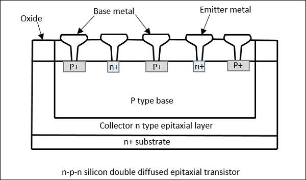
Construction of Microwave Transistors
An n type epitaxial layer is grown on n+ substrate that constitutes the collector. On this n region, a SiO2 layer is grown thermally. A p-base and heavily doped n-emitters are diffused into the base. Openings are made in Oxide for Ohmic contacts. Connections are made in parallel.
Such transistors have a surface geometry categorized as either interdigitated, overlay, or matrix. These forms are shown in the following figure.
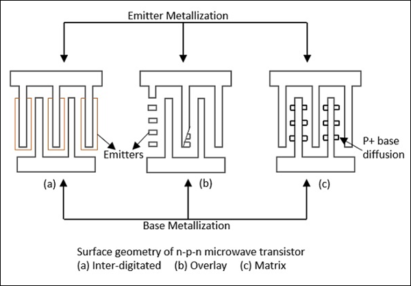
Power transistors employ all the three surface geometries.
Small signal transistors employ interdigitated surface geometry. Interdigitated structure is suitable for small signal applications in the L, S, and C bands.
The matrix geometry is sometimes called mesh or emitter grid. Overlay and Matrix structures are useful as power devices in the UHF and VHF regions.
Operation of Microwave Transistors
In a microwave transistor, initially the emitter-base and collector-base junctions are reverse biased. On the application of a microwave signal, the emitter-base junction becomes forward biased. If a p-n-p transistor is considered, the application of positive peak of signal, forward biases the emitter-base junction, making the holes to drift to the thin negative base. The holes further accelerate to the negative terminal of the bias voltage between the collector and the base terminals. A load connected at the collector, receives a current pulse.
Solid State Devices
The classification of solid state Microwave devices can be done −
Depending upon their electrical behavior
-
Non-linear resistance type.
Example − Varistors (variable resistances)
-
Non-Linear reactance type.
Example − Varactors (variable reactors)
-
Negative resistance type.
Example − Tunnel diode, Impatt diode, Gunn diode
-
Controllable impedance type.
Example − PIN diode
-
- Depending upon their construction
- Point contact diodes
- Schottky barrier diodes
- Metal Oxide Semiconductor devices (MOS)
- Metal insulation devices
The types of diodes which we have mentioned here have many uses such as amplification, detection, power generation, phase shifting, down conversion, up conversion, limiting modulation, switching, etc.
Varactor Diode
A voltage variable capacitance of a reverse biased junction can be termed as a Varactor diode. Varactor diode is a semi-conductor device in which the junction capacitance can be varied as a function of the reverse bias of the diode. The CV characteristics of a typical Varactor diode and its symbols are shown in the following figure.
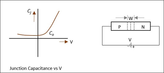
The junction capacitance depends on the applied voltage and junction design. We know that,
$$C_j \: \alpha \: V_{r}^{-n}$$
Where
$C_j$ = Junction capacitance
$V_r$ = Reverse bias voltage
$n$ = A parameter that decides the type of junction
If the junction is reverse biased, the mobile carriers deplete the junction, resulting in some capacitance, where the diode behaves as a capacitor, with the junction acting as a dielectric. The capacitance decreases with the increase in reverse bias.
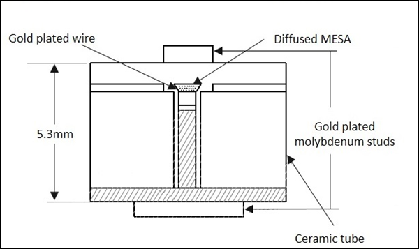
The encapsulation of diode contains electrical leads which are attached to the semiconductor wafer and a lead attached to the ceramic case. The following figure shows how a microwave Varactor diode looks.
These are capable of handling large powers and large reverse breakdown voltages. These have low noise. Although variation in junction capacitance is an important factor in this diode, parasitic resistances, capacitances, and conductances are associated with every practical diode, which should be kept low.
Applications of Varactor Diode
Varactor diodes are used in the following applications −
- Up conversion
- Parametric amplifier
- Pulse generation
- Pulse shaping
- Switching circuits
- Modulation of microwave signals
Schottky Barrier Diode
This is a simple diode that exhibits non-linear impedance. These diodes are mostly used for microwave detection and mixing.
Construction of Schottky Barrier Diode
A semi-conductor pellet is mounted on a metal base. A spring loaded wire is connected with a sharp point to this silicon pellet. This can be easily mounted into coaxial or waveguide lines. The following figure gives a clear picture of the construction.
Operation of Schottky Barrier Diode
With the contact between the semi-conductor and the metal, a depletion region is formed. The metal region has smaller depletion width, comparatively. When contact is made, electron flow occurs from the semi-conductor to the metal. This depletion builds up a positive space charge in the semi-conductor and the electric field opposes further flow, which leads to the creation of a barrier at the interface.
During forward bias, the barrier height is reduced and the electrons get injected into the metal, whereas during reverse bias, the barrier height increases and the electron injection almost stops.
Advantages of Schottky Barrier Diode
These are the following advantages.
- Low cost
- Simplicity
- Reliable
- Noise figures 4 to 5dB
Applications of Schottky Barrier Diode
These are the following applications.
- Low noise mixer
- Balanced mixer in continuous wave radar
- Microwave detector
Gunn Effect Devices
J B Gunn discovered periodic fluctuations of current passing through the n-type GaAs specimen when the applied voltage exceeded a certain critical value. In these diodes, there are two valleys, L & U valleys in conduction band and the electron transfer occurs between them, depending upon the applied electric field. This effect of population inversion from lower L-valley to upper U-valley is called Transfer Electron Effect and hence these are called as Transfer Electron Devices (TEDs).
Applications of Gunn Diodes
Gunn diodes are extensively used in the following devices −
- Radar transmitters
- Transponders in air traffic control
- Industrial telemetry systems
- Power oscillators
- Logic circuits
- Broadband linear amplifier
Avalanche Transit Time Devices
The process of having a delay between voltage and current, in avalanche together with transit time, through the material is said to be Negative resistance. The devices that helps to make a diode exhibit this property are called as Avalanche transit time devices.
The examples of the devices that come under this category are IMPATT, TRAPATT and BARITT diodes. Let us take a look at each of them, in detail.
IMPATT Diode
This is a high-power semiconductor diode, used in high frequency microwave applications. The full form IMPATT is IMPact ionization Avalanche Transit Time diode.
A voltage gradient when applied to the IMPATT diode, results in a high current. A normal diode will eventually breakdown by this. However, IMPATT diode is developed to withstand all this. A high potential gradient is applied to back bias the diode and hence minority carriers flow across the junction.
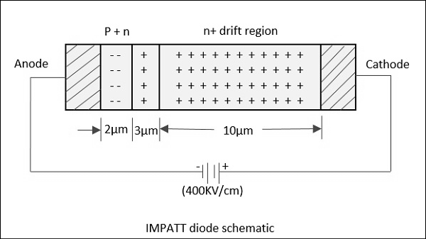
Application of a RF AC voltage if superimposed on a high DC voltage, the increased velocity of holes and electrons results in additional holes and electrons by thrashing them out of the crystal structure by Impact ionization. If the original DC field applied was at the threshold of developing this situation, then it leads to the avalanche current multiplication and this process continues. This can be understood by the following figure.
Due to this effect, the current pulse takes a phase shift of 90°. However, instead of being there, it moves towards cathode due to the reverse bias applied. The time taken for the pulse to reach cathode depends upon the thickness of n+ layer, which is adjusted to make it 90° phase shift. Now, a dynamic RF negative resistance is proved to exist. Hence, IMPATT diode acts both as an oscillator and an amplifier.
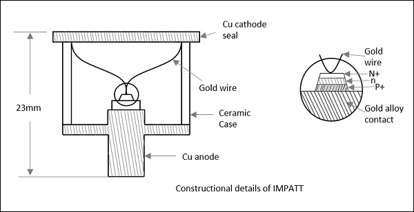
The following figure shows the constructional details of an IMPATT diode.
The efficiency of IMPATT diode is represented as
$$\eta = \left [ \frac{P_{ac}}{P_{dc}} \right ] = \frac{V_a}{V_d}\left [ \frac{I_a}{I_d} \right ]$$
Where,
$P_{ac}$ = AC power
$P_{dc}$ = DC power
$V_a \: \& \: I_a$ = AC voltage & current
$V_d \: \& \: I_d$ = DC voltage & current
Disadvantages
Following are the disadvantages of IMPATT diode.
- It is noisy as avalanche is a noisy process
- Tuning range is not as good as in Gunn diodes
Applications
Following are the applications of IMPATT diode.
- Microwave oscillator
- Microwave generators
- Modulated output oscillator
- Receiver local oscillator
- Negative resistance amplifications
- Intrusion alarm networks (high Q IMPATT)
- Police radar (high Q IMPATT)
- Low power microwave transmitter (high Q IMPATT)
- FM telecom transmitter (low Q IMPATT)
- CW Doppler radar transmitter (low Q IMPATT)
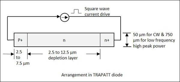
TRAPATT Diode
The full form of TRAPATT diode is TRApped Plasma Avalanche Triggered Transit diode. A microwave generator which operates between hundreds of MHz to GHz. These are high peak power diodes usually n+- p-p+ or p+-n-n+ structures with n-type depletion region, width varying from 2.5 to 1.25 m. The following figure depicts this.
The electrons and holes trapped in low field region behind the zone, are made to fill the depletion region in the diode. This is done by a high field avalanche region which propagates through the diode.
The following figure shows a graph in which AB shows charging, BC shows plasma formation, DE shows plasma extraction, EF shows residual extraction, and FG shows charging.
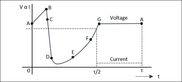
Let us see what happens at each of the points.
A: The voltage at point A is not sufficient for the avalanche breakdown to occur. At A, charge carriers due to thermal generation results in charging of the diode like a linear capacitance.
A-B: At this point, the magnitude of the electric field increases. When a sufficient number of carriers are generated, the electric field is depressed throughout the depletion region causing the voltage to decrease from B to C.
C: This charge helps the avalanche to continue and a dense plasma of electrons and holes is created. The field is further depressed so as not to let the electrons or holes out of the depletion layer, and traps the remaining plasma.
D: The voltage decreases at point D. A long time is required to clear the plasma as the total plasma charge is large compared to the charge per unit time in the external current.
E: At point E, the plasma is removed. Residual charges of holes and electrons remain each at one end of the deflection layer.
E to F: The voltage increases as the residual charge is removed.
F: At point F, all the charge generated internally is removed.
F to G: The diode charges like a capacitor.
G: At point G, the diode current comes to zero for half a period. The voltage remains constant as shown in the graph above. This state continues until the current comes back on and the cycle repeats.
The avalanche zone velocity $V_s$ is represented as
$$V_s = \frac{dx}{dt} = \frac{J}{qN_A}$$
Where
$J$ = Current density
$q$ = Electron charge 1.6 x 10⁻¹⁹
$N_A$ = Doping concentration
The avalanche zone will quickly sweep across most of the diode and the transit time of the carriers is represented as
$$\tau_s = \frac{L}{V_s}$$
Where
$V_s$ = Saturated carrier drift velocity
$L$ = Length of the specimen
The transit time calculated here is the time between the injection and the collection. The repeated action increases the output to make it an amplifier, whereas a microwave low pass filter connected in shunt with the circuit can make it work as an oscillator.
Applications
There are many applications of this diode.
- Low power Doppler radars
- Local oscillator for radars
- Microwave beacon landing system
- Radio altimeter
- Phased array radar, etc.
BARITT Diode
The full form of BARITT Diode is BARrier Injection Transit Time diode. These are the latest invention in this family. Though these diodes have long drift regions like IMPATT diodes, the carrier injection in BARITT diodes is caused by forward biased junctions, but not from the plasma of an avalanche region as in them.
In IMPATT diodes, the carrier injection is quite noisy due to the impact ionization. In BARITT diodes, to avoid the noise, carrier injection is provided by punch through of the depletion region. The negative resistance in a BARITT diode is obtained on account of the drift of the injected holes to the collector end of the diode, made of p-type material.
The following figure shows the constructional details of a BARITT diode.
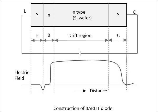
For a m-n-m BARITT diode, Ps-Si Schottky barrier contacts metals with n-type Si wafer in between. A rapid increase in current with applied voltage (above 30v) is due to the thermionic hole injection into the semiconductor.
The critical voltage $(Vc)$ depends on the doping constant $(N)$, length of the semiconductor $(L)$ and the semiconductor dielectric permittivity $(\epsilon S)$ represented as
$$V_c = \frac{qNL^2}{2\epsilon S}$$
Monolithic Microwave Integrated Circuit (MMIC)
Microwave ICs are the best alternative to conventional waveguide or coaxial circuits, as they are low in weight, small in size, highly reliable and reproducible. The basic materials used for monolithic microwave integrated circuits are −
- Substrate material
- Conductor material
- Dielectric films
- Resistive films
These are so chosen to have ideal characteristics and high efficiency. The substrate on which circuit elements are fabricated is important as the dielectric constant of the material should be high with low dissipation factor, along with other ideal characteristics. The substrate materials used are GaAs, Ferrite/garnet, Aluminum, beryllium, glass and rutile.
The conductor material is so chosen to have high conductivity, low temperature coefficient of resistance, good adhesion to substrate and etching, etc. Aluminum, copper, gold, and silver are mainly used as conductor materials. The dielectric materials and resistive materials are so chosen to have low loss and good stability.
Fabrication Technology
In hybrid integrated circuits, the semiconductor devices and passive circuit elements are formed on a dielectric substrate. The passive circuits are either distributed or lumped elements, or a combination of both.
Hybrid integrated circuits are of two types.
- Hybrid IC
- Miniature Hybrid IC
In both the above processes, Hybrid IC uses the distributed circuit elements that are fabricated on IC using a single layer metallization technique, whereas Miniature hybrid IC uses multi-level elements.
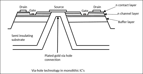
Most analog circuits use meso-isolation technology to isolate active n-type areas used for FETs and diodes. Planar circuits are fabricated by implanting ions into semi-insulating substrate, and to provide isolation the areas are masked off.
"Via hole" technology is used to connect the source with source electrodes connected to the ground, in a GaAs FET, which is shown in the following figure.
There are many applications of MMICs.
- Military communication
- Radar
- ECM
- Phased array antenna systems
- Spread spectrum and TDMA systems
They are cost-effective and also used in many domestic consumer applications such as DTH, telecom and instrumentation, etc.
Microwave Engineering - Microwave Devices
Just like other systems, the Microwave systems consists of many Microwave components, mainly with source at one end and load at the other, which are all connected with waveguides or coaxial cable or transmission line systems.
Following are the properties of waveguides.
- High SNR
- Low attenuation
- Lower insertion loss
Waveguide Microwave Functions
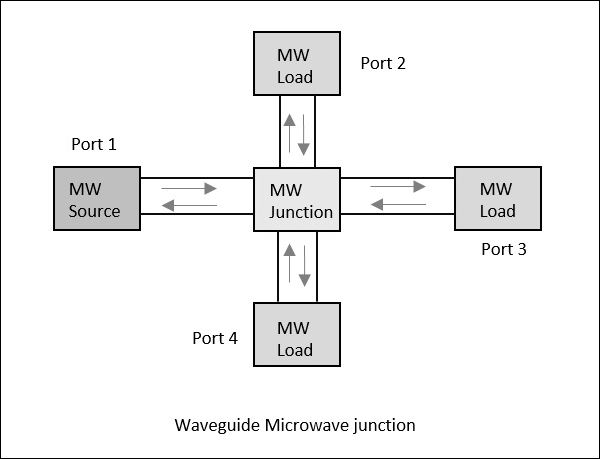
Consider a waveguide having 4 ports. If the power is applied to one port, it goes through all the 3 ports in some proportions where some of it might reflect back from the same port. This concept is clearly depicted in the following figure.
Scattering Parameters
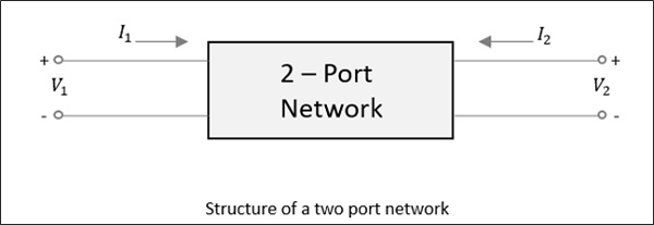
For a two-port network, as shown in the following figure, if the power is applied at one port, as we just discussed, most of the power escapes from the other port, while some of it reflects back to the same port. In the following figure, if V1 or V2 is applied, then I1 or I2 current flows respectively.
If the source is applied to the opposite port, another two combinations are to be considered. So, for a two-port network, 2 × 2 = 4 combinations are likely to occur.
The travelling waves with associated powers when scatter out through the ports, the Microwave junction can be defined by S-Parameters or Scattering Parameters, which are represented in a matrix form, called as "Scattering Matrix".
Scattering Matrix
It is a square matrix which gives all the combinations of power relationships between the various input and output ports of a Microwave junction. The elements of this matrix are called "Scattering Coefficients" or "Scattering (S) Parameters".
Consider the following figure.
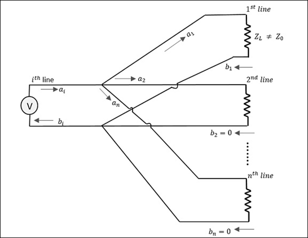
Here, the source is connected through $i^{th}$ line while $a_1$ is the incident wave and $b_1$ is the reflected wave.
If a relation is given between $b_1$ and $a_1$,
$$b_1 = (reflection \: \: coefficient)a_1 = S_{1i}a_1$$
Where
$S_{1i}$ = Reflection coefficient of $1^{st}$ line (where $i$ is the input port and $1$ is the output port)
$1$ = Reflection from $1^{st}$ line
$i$ = Source connected at $i^{th}$ line
If the impedance matches, then the power gets transferred to the load. Unlikely, if the load impedance doesn't match with the characteristic impedance. Then, the reflection occurs. That means, reflection occurs if
$$Z_l \neq Z_o$$
However, if this mismatch is there for more than one port, example $'n'$ ports, then $i = 1$ to $n$ (since $i$ can be any line from $1$ to $n$).
Therefore, we have
$$b_1 = S_{11}a_1 + S_{12}a_2 + S_{13}a_3 + ............... + S_{1n}a_n$$
$$b_2 = S_{21}a_1 + S_{22}a_2 + S_{23}a_3 + ............... + S_{2n}a_n$$
$$.$$
$$.$$
$$.$$
$$.$$
$$.$$
$$b_n = S_{n1}a_1 + S_{n2}a_2 + S_{n3}a_3 + ............... + S_{nn}a_n$$
When this whole thing is kept in a matrix form,
$$\begin{bmatrix} b_1\\ b_2\\ b_3\\ .\\ .\\ .\\ b_n \end{bmatrix} = \begin{bmatrix} S_{11}& S_{12}& S_{13}& ...& S_{1n}\\ S_{21}& S_{22}& S_{23}& ...& S_{2n}\\ .& .& .& ...& . \\ .& .& .& ...& . \\ .& .& .& ...& . \\ S_{n1}& S_{n2}& S_{n3}& ...& S_{nn}\\ \end{bmatrix} \times \begin{bmatrix} a_1\\ a_2\\ a_3\\ .\\ .\\ .\\ a_n \end{bmatrix}$$
Column matrix $[b]$ Scattering matrix $[S]$Matrix $[a]$
The column matrix $\left [ b \right ]$ corresponds to the reflected waves or the output, while the matrix $\left [ a \right ]$ corresponds to the incident waves or the input. The scattering column matrix $\left [ s \right ]$ which is of the order of $n \times n$ contains the reflection coefficients and transmission coefficients. Therefore,
$$\left [ b \right ] = \left [ S \right ]\left [ a \right ]$$
Properties of [S] Matrix
The scattering matrix is indicated as $[S]$ matrix. There are few standard properties for $[S]$ matrix. They are −
-
$[S]$ is always a square matrix of order (nxn)
$[S]_{n \times n}$
-
$[S]$ is a symmetric matrix
i.e., $S_{ij} = S_{ji}$
-
$[S]$ is a unitary matrix
i.e., $[S][S]^* = I$
The sum of the products of each term of any row or column multiplied by the complex conjugate of the corresponding terms of any other row or column is zero. i.e.,
$$\sum_{i=j}^{n} S_{ik} S_{ik}^{*} = 0 \: for \: k \neq j$$
$$( k = 1,2,3, ... \: n ) \: and \: (j = 1,2,3, ... \: n)$$
-
If the electrical distance between some $k^{th}$ port and the junction is $\beta _kI_k$, then the coefficients of $S_{ij}$ involving $k$, will be multiplied by the factor $e^{-j\beta kIk}$
In the next few chapters, we will take a look at different types of Microwave Tee junctions.
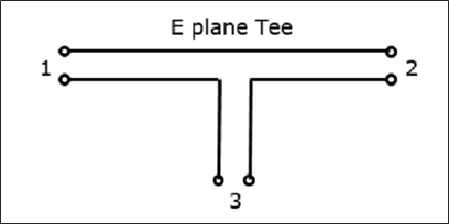
Microwave Engineering - E-Plane Tee
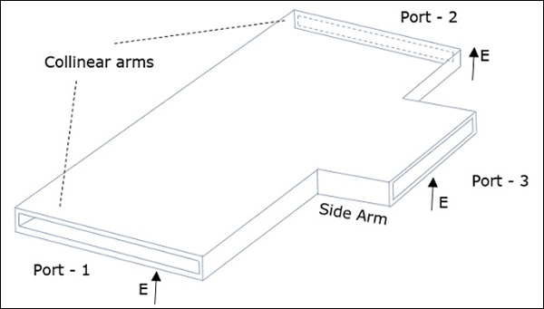
An E-Plane Tee junction is formed by attaching a simple waveguide to the broader dimension of a rectangular waveguide, which already has two ports. The arms of rectangular waveguides make two ports called collinear ports i.e., Port1 and Port2, while the new one, Port3 is called as Side arm or E-arm. T his E-plane Tee is also called as Series Tee.
As the axis of the side arm is parallel to the electric field, this junction is called E-Plane Tee junction. This is also called as Voltage or Series junction. The ports 1 and 2 are 180° out of phase with each other. The cross-sectional details of E-plane tee can be understood by the following figure.
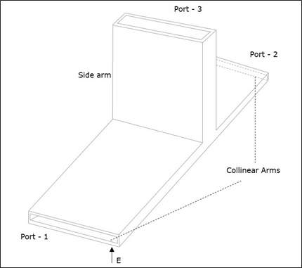
The following figure shows the connection made by the sidearm to the bi-directional waveguide to form the parallel port.
Properties of E-Plane Tee
The properties of E-Plane Tee can be defined by its $[S]_{3x3}$ matrix.
It is a 3×3 matrix as there are 3 possible inputs and 3 possible outputs.
$[S] = \begin{bmatrix} S_{11}& S_{12}& S_{13}\\ S_{21}& S_{22}& S_{23}\\ S_{31}& S_{32}& S_{33} \end{bmatrix}$ ........ Equation 1
Scattering coefficients $S_{13}$ and $S_{23}$ are out of phase by 180° with an input at port 3.
$S_{23} = -S_{13}$........ Equation 2
The port is perfectly matched to the junction.
$S_{33} = 0$........ Equation 3
From the symmetric property,
$S_{ij} = S_{ji}$
$S_{12} = S_{21} \: \: S_{23} = S_{32} \: \: S_{13} = S_{31}$........ Equation 4
Considering equations 3 & 4, the $[S]$ matrix can be written as,
$[S] = \begin{bmatrix} S_{11}& S_{12}& S_{13}\\ S_{12}& S_{22}& -S_{13}\\ S_{13}& -S_{13}& 0 \end{bmatrix}$........ Equation 5
We can say that we have four unknowns, considering the symmetry property.
From the Unitary property
$$[S][S]\ast = [I]$$
$$\begin{bmatrix} S_{11}& S_{12}& S_{13}\\ S_{12}& S_{22}& -S_{13}\\ S_{13}& -S_{13}& 0 \end{bmatrix} \: \begin{bmatrix} S_{11}^{*}& S_{12}^{*}& S_{13}^{*}\\ S_{12}^{*}& S_{22}^{*}& -S_{13}^{*}\\ S_{13}^{*}& -S_{13}^{*}& 0 \end{bmatrix} = \begin{bmatrix} 1& 0& 0\\ 0& 1& 0\\ 0& 0& 1 \end{bmatrix}$$
Multiplying we get,
(Noting R as row and C as column)
$R_1C_1 : S_{11}S_{11}^{*} + S_{12}S_{12}^{*} + S_{13}S_{13}^{*} = 1$
$\left | S_{11} \right |^2 + \left | S_{11} \right |^2 + \left | S_{11} \right |^2 = 1$ ........ Equation 6
$R_2C_2 : \left | S_{12} \right |^2 + \left | S_{22} \right |^2 + \left | S_{13} \right |^2 = 1$ ......... Equation 7
$R_3C_3 : \left | S_{13} \right |^2 + \left | S_{13} \right |^2 = 1$ ......... Equation 8
$R_3C_1 : S_{13}S_{11}^{*} - S_{13}S_{12}^{*} = 1$ ......... Equation 9
Equating the equations 6 & 7, we get
$S_{11} = S_{22} $ ......... Equation 10
From Equation 8,
$2\left | S_{13} \right |^2 \quad or \quad S_{13} = \frac{1}{\sqrt{2}}$ ......... Equation 11
From Equation 9,
$S_{13}\left ( S_{11}^{*} - S_{12}^{*} \right )$
Or $S_{11} = S_{12} = S_{22}$ ......... Equation 12
Using the equations 10, 11, and 12 in the equation 6,
we get,
$\left | S_{11} \right |^2 + \left | S_{11} \right |^2 + \frac{1}{2} = 1$
$2\left | S_{11} \right |^2 = \frac{1}{2}$
Or $S_{11} = \frac{1}{2}$ ......... Equation 13
Substituting the values from the above equations in $[S]$ matrix,
We get,
$$\left [ S \right ] = \begin{bmatrix} \frac{1}{2}& \frac{1}{2}& \frac{1}{\sqrt{2}}\\ \frac{1}{2}& \frac{1}{2}& -\frac{1}{\sqrt{2}}\\ \frac{1}{\sqrt{2}}& -\frac{1}{\sqrt{2}}& 0 \end{bmatrix}$$
We know that $[b]$ = $[S] [a]$
$$\begin{bmatrix}b_1 \\ b_2 \\ b_3 \end{bmatrix} = \begin{bmatrix} \frac{1}{2}& \frac{1}{2}& \frac{1}{\sqrt{2}}\\ \frac{1}{2}& \frac{1}{2}& -\frac{1}{\sqrt{2}}\\ \frac{1}{\sqrt{2}}& -\frac{1}{\sqrt{2}}& 0 \end{bmatrix} \begin{bmatrix} a_1\\ a_2\\ a_3 \end{bmatrix}$$
This is the scattering matrix for E-Plane Tee, which explains its scattering properties.
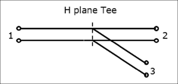
Microwave Engineering - H-Plane Tee
An H-Plane Tee junction is formed by attaching a simple waveguide to a rectangular waveguide which already has two ports. The arms of rectangular waveguides make two ports called collinear ports i.e., Port1 and Port2, while the new one, Port3 is called as Side arm or H-arm. This H-plane Tee is also called as Shunt Tee.
As the axis of the side arm is parallel to the magnetic field, this junction is called H-Plane Tee junction. This is also called as Current junction, as the magnetic field divides itself into arms. The cross-sectional details of H-plane tee can be understood by the following figure.
The following figure shows the connection made by the sidearm to the bi-directional waveguide to form the serial port.
Properties of H-Plane Tee
The properties of H-Plane Tee can be defined by its $\left [ S \right ]_{3\times 3}$ matrix.
It is a 3×3 matrix as there are 3 possible inputs and 3 possible outputs.
$[S] = \begin{bmatrix} S_{11}& S_{12}& S_{13}\\ S_{21}& S_{22}& S_{23}\\ S_{31}& S_{32}& S_{33} \end{bmatrix}$ ........ Equation 1
Scattering coefficients $S_{13}$ and $S_{23}$ are equal here as the junction is symmetrical in plane.
From the symmetric property,
$S_{ij} = S_{ji}$
$S_{12} = S_{21} \: \: S_{23} = S_{32} = S_{13} \: \: S_{13} = S_{31}$
The port is perfectly matched
$S_{33} = 0$
Now, the $[S]$ matrix can be written as,
$[S] = \begin{bmatrix} S_{11}& S_{12}& S_{13}\\ S_{12}& S_{22}& S_{13}\\ S_{13}& S_{13}& 0 \end{bmatrix}$ ........ Equation 2
We can say that we have four unknowns, considering the symmetry property.
From the Unitary property
$$[S][S]\ast = [I]$$
$$\begin{bmatrix} S_{11}& S_{12}& S_{13}\\ S_{12}& S_{22}& S_{13}\\ S_{13}& S_{13}& 0 \end{bmatrix} \: \begin{bmatrix} S_{11}^{*}& S_{12}^{*}& S_{13}^{*}\\ S_{12}^{*}& S_{22}^{*}& S_{13}^{*}\\ S_{13}^{*}& S_{13}^{*}& 0 \end{bmatrix} = \begin{bmatrix} 1& 0& 0\\ 0& 1& 0\\ 0& 0& 1 \end{bmatrix}$$
Multiplying we get,
(Noting R as row and C as column)
$R_1C_1 : S_{11}S_{11}^{*} + S_{12}S_{12}^{*} + S_{13}S_{13}^{*} = 1$
$\left | S_{11} \right |^2 + \left | S_{12} \right |^2 + \left | S_{13} \right |^2 = 1$ ........ Equation 3
$R_2C_2 : \left | S_{12} \right |^2 + \left | S_{22} \right |^2 + \left | S_{13} \right |^2 = 1$ ......... Equation 4
$R_3C_3 : \left | S_{13} \right |^2 + \left | S_{13} \right |^2 = 1$ ......... Equation 5
$R_3C_1 : S_{13}S_{11}^{*} - S_{13}S_{12}^{*} = 0$ ......... Equation 6
$2\left | S_{13} \right |^2 = 1 \quad or \quad S_{13} = \frac{1}{\sqrt{2}}$ ......... Equation 7
$\left | S_{11} \right |^2 = \left | S_{22} \right |^2$
$S_{11} = S_{22}$ ......... Equation 8
From the Equation 6,$S_{13}\left ( S_{11}^{*} + S_{12}^{*} \right ) = 0$
Since, $S_{13} \neq 0, S_{11}^{*} + S_{12}^{*} = 0, \: or \: S_{11}^{*} = -S_{12}^{*}$
Or $S_{11} = -S_{12} \:\: or \:\: S_{12} = -S_{11}$......... Equation 9
Using these in equation 3,
Since, $S_{13} \neq 0, S_{11}^{*} + S_{12}^{*} = 0, \: or \: S_{11}^{*} = -S_{12}^{*}$
$\left | S_{11} \right |^2 + \left | S_{11} \right |^2 + \frac{1}{2} = 1 \quad or \quad 2\left | S_{11} \right |^2 = \frac{1}{2} \quad or \quad S_{11} = \frac{1}{2}$..... Equation 10
From equation 8 and 9,
$S_{12} = -\frac{1}{2}$......... Equation 11
$S_{22} = \frac{1}{2}$......... Equation 12
Substituting for $S_{13}$, $S_{11}$, $S_{12}$ and $S_{22}$ from equation 7 and 10, 11 and 12 in equation 2,
We get,
$$\left [ S \right ] = \begin{bmatrix} \frac{1}{2}& -\frac{1}{2}& \frac{1}{\sqrt{2}}\\ -\frac{1}{2}& \frac{1}{2}& \frac{1}{\sqrt{2}}\\ \frac{1}{\sqrt{2}}& \frac{1}{\sqrt{2}}& 0 \end{bmatrix}$$
We know that $[b]$ = $[s] [a]$
$$\begin{bmatrix}b_1 \\ b_2 \\ b_3 \end{bmatrix} = \begin{bmatrix} \frac{1}{2}& -\frac{1}{2}& \frac{1}{\sqrt{2}}\\ -\frac{1}{2}& \frac{1}{2}& \frac{1}{\sqrt{2}}\\ \frac{1}{\sqrt{2}}& \frac{1}{\sqrt{2}}& 0 \end{bmatrix} \begin{bmatrix} a_1\\ a_2\\ a_3 \end{bmatrix}$$
This is the scattering matrix for H-Plane Tee, which explains its scattering properties.
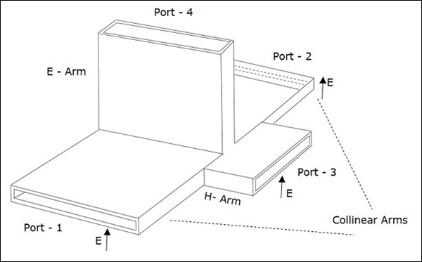
Microwave Engineering - E-H Plane Tee
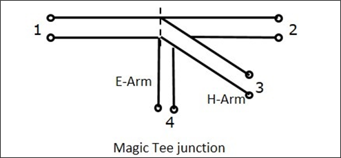
An E-H Plane Tee junction is formed by attaching two simple waveguides one parallel and the other series, to a rectangular waveguide which already has two ports. This is also called as Magic Tee, or Hybrid or 3dB coupler.
The arms of rectangular waveguides make two ports called collinear ports i.e., Port 1 and Port 2, while the Port 3 is called as H-Arm or Sum port or Parallel port. Port 4 is called as E-Arm or Difference port or Series port.
The cross-sectional details of Magic Tee can be understood by the following figure.
The following figure shows the connection made by the side arms to the bi-directional waveguide to form both parallel and serial ports.
Characteristics of E-H Plane Tee
If a signal of equal phase and magnitude is sent to port 1 and port 2, then the output at port 4 is zero and the output at port 3 will be the additive of both the ports 1 and 2.
If a signal is sent to port 4, (E-arm) then the power is divided between port 1 and 2 equally but in opposite phase, while there would be no output at port 3. Hence, $S_{34}$ = 0.
If a signal is fed at port 3, then the power is divided between port 1 and 2 equally, while there would be no output at port 4. Hence, $S_{43}$ = 0.
If a signal is fed at one of the collinear ports, then there appears no output at the other collinear port, as the E-arm produces a phase delay and the H-arm produces a phase advance. So, $S_{12}$ = $S_{21}$ = 0.
Properties of E-H Plane Tee
The properties of E-H Plane Tee can be defined by its $\left [ S \right ]_{4\times 4}$ matrix.
It is a 4×4 matrix as there are 4 possible inputs and 4 possible outputs.
$[S] = \begin{bmatrix} S_{11}& S_{12}& S_{13}& S_{14}\\ S_{21}& S_{22}& S_{23}& S_{24}\\ S_{31}& S_{32}& S_{33}& S_{34}\\ S_{41}& S_{42}& S_{43}& S_{44} \end{bmatrix}$ ........ Equation 1
As it has H-Plane Tee section
$S_{23} = S_{13}$........ Equation 2
As it has E-Plane Tee section
$S_{24} = -S_{14}$........ Equation 3
The E-Arm port and H-Arm port are so isolated that the other won't deliver an output, if an input is applied at one of them. Hence, this can be noted as
$S_{34} = S_{43} = 0$........ Equation 4
From the symmetry property, we have
$S_{ij} = S_{ji}$
$S_{12} = S_{21}, S_{13} = S_{31}, S_{14} = S_{41}$
$S_{23} = S_{32}, S_{24} = S_{42}, S_{34} = S_{43}$........ Equation 5
If the ports 3 and 4 are perfectly matched to the junction, then
$S_{33} = S_{44} = 0$........ Equation 6
Substituting all the above equations in equation 1, to obtain the $[S]$ matrix,
$[S] = \begin{bmatrix} S_{11}& S_{12}& S_{13}& S_{14}\\ S_{12}& S_{22}& S_{13}& -S_{14}\\ S_{13}& S_{13}& 0& 0\\ S_{14}& -S_{14}& 0& 0 \end{bmatrix}$........ Equation 7
From Unitary property, $[S][S]^\ast = [I]$
$\begin{bmatrix} S_{11}& S_{12}& S_{13}& S_{14}\\ S_{12}& S_{22}& S_{13}& -S_{14}\\ S_{13}& S_{13}& 0& 0\\ S_{14}& -S_{14}& 0& 0 \end{bmatrix} \begin{bmatrix} S_{11}^{*}& S_{12}^{*}& S_{13}^{*}& S_{14}^{*}\\ S_{12}^{*}& S_{22}^{*}& S_{13}^{*}& -S_{14}^{*}\\ S_{13}& S_{13}& 0& 0\\ S_{14}& -S_{14}& 0& 0 \end{bmatrix}$
$ = \begin{bmatrix} 1& 0& 0& 0\\ 0& 1& 0& 0\\ 0& 0& 1& 0\\ 0& 0& 0& 1 \end{bmatrix}$
$R_1C_1 : \left | S_{11} \right |^2 + \left | S_{12} \right |^2 + \left | S_{13} \right |^2 = 1 + \left | S_{14} \right |^2 = 1$ ......... Equation 8
$R_2C_2 : \left | S_{12} \right |^2 + \left | S_{22} \right |^2 + \left | S_{13} \right |^2 = 1 + \left | S_{14} \right |^2 = 1$ ......... Equation 9
$R_3C_3 : \left | S_{13} \right |^2 + \left | S_{13} \right |^2 = 1$ ......... Equation 10
$R_4C_4 : \left | S_{14} \right |^2 + \left | S_{14} \right |^2 = 1$ ......... Equation 11
From the equations 10 and 11, we get
$S_{13} = \frac{1}{\sqrt{2}}$........ Equation 12
$S_{14} = \frac{1}{\sqrt{2}}$........ Equation 13
Comparing the equations 8 and 9, we have
$S_{11} = S_{22}$ ......... Equation 14
Using these values from the equations 12 and 13, we get
$\left | S_{11} \right |^2 + \left | S_{12} \right |^2 + \frac{1}{2} + \frac{1}{2} = 1$
$\left | S_{11} \right |^2 + \left | S_{12} \right |^2 = 0$
$S_{11} = S_{22} = 0$ ......... Equation 15
From equation 9, we get $S_{22} = 0$ ......... Equation 16
Now we understand that ports 1 and 2 are perfectly matched to the junction. As this is a 4 port junction, whenever two ports are perfectly matched, the other two ports are also perfectly matched to the junction.
The junction where all the four ports are perfectly matched is called as Magic Tee Junction.
By substituting the equations from 12 to 16, in the $[S]$ matrix of equation 7, we obtain the scattering matrix of Magic Tee as
$$[S] = \begin{bmatrix} 0& 0& \frac{1}{2}& \frac{1}{\sqrt{2}}\\ 0& 0& \frac{1}{2}& -\frac{1}{\sqrt{2}}\\ \frac{1}{\sqrt{2}}& \frac{1}{\sqrt{2}}& 0& 0\\ \frac{1}{\sqrt{2}}& -\frac{1}{\sqrt{2}}& 0& 0 \end{bmatrix}$$
We already know that, $[b]$ = $[S] [a]$
Rewriting the above, we get
$$\begin{vmatrix} b_1\\ b_2\\ b_3\\ b_4 \end{vmatrix} = \begin{bmatrix} 0& 0& \frac{1}{2}& \frac{1}{\sqrt{2}}\\ 0& 0& \frac{1}{2}& -\frac{1}{\sqrt{2}}\\ \frac{1}{\sqrt{2}}& \frac{1}{\sqrt{2}}& 0& 0\\ \frac{1}{\sqrt{2}}& -\frac{1}{\sqrt{2}}& 0& 0 \end{bmatrix} \begin{vmatrix} a_1\\ a_2\\ a_3\\ a_4 \end{vmatrix}$$
Applications of E-H Plane Tee
Some of the most common applications of E-H Plane Tee are as follows −
E-H Plane junction is used to measure the impedance − A null detector is connected to E-Arm port while the Microwave source is connected to H-Arm port. The collinear ports together with these ports make a bridge and the impedance measurement is done by balancing the bridge.
E-H Plane Tee is used as a duplexer − A duplexer is a circuit which works as both the transmitter and the receiver, using a single antenna for both purposes. Port 1 and 2 are used as receiver and transmitter where they are isolated and hence will not interfere. Antenna is connected to E-Arm port. A matched load is connected to H-Arm port, which provides no reflections. Now, there exists transmission or reception without any problem.
E-H Plane Tee is used as a mixer − E-Arm port is connected with antenna and the H-Arm port is connected with local oscillator. Port 2 has a matched load which has no reflections and port 1 has the mixer circuit, which gets half of the signal power and half of the oscillator power to produce IF frequency.
In addition to the above applications, an E-H Plane Tee junction is also used as Microwave bridge, Microwave discriminator, etc.
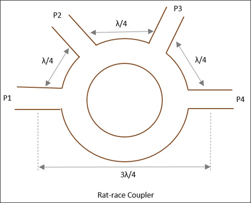
Microwave Engineering - Rat-race Junction
This microwave device is used when there is a need to combine two signals with no phase difference and to avoid the signals with a path difference.
A normal three-port Tee junction is taken and a fourth port is added to it, to make it a ratrace junction. All of these ports are connected in angular ring forms at equal intervals using series or parallel junctions.
The mean circumference of total race is 1.5λ and each of the four ports are separated by a distance of λ/4. The following figure shows the image of a Rat-race junction.
Let us consider a few cases to understand the operation of a Rat-race junction.
Case 1
If the input power is applied at port 1, it gets equally split into two ports, but in clockwise direction for port 2 and anti-clockwise direction for port 4. Port 3 has absolutely no output.
The reason being, at ports 2 and 4, the powers combine in phase, whereas at port 3, cancellation occurs due to λ/2 path difference.
Case 2
If the input power is applied at port 3, the power gets equally divided between port 2 and port 4. But there will be no output at port 1.
Case 3
If two unequal signals are applied at port 1 itself, then the output will be proportional to the sum of the two input signals, which is divided between port 2 and 4. Now at port 3, the differential output appears.
The Scattering Matrix for Rat-race junction is represented as
$$[S] = \begin{bmatrix} 0& S_{12}& 0& S_{14}\\ S_{21}& 0& S_{23}& 0\\ 0& S_{32}& 0& S_{34}\\ S_{41}& 0& S_{43}& 0 \end{bmatrix}$$
Applications
Rat-race junction is used for combining two signals and dividing a signal into two halves.
Microwave Engineering - Directional Couplers
A Directional coupler is a device that samples a small amount of Microwave power for measurement purposes. The power measurements include incident power, reflected power, VSWR values, etc.
Directional Coupler is a 4-port waveguide junction consisting of a primary main waveguide and a secondary auxiliary waveguide. The following figure shows the image of a directional coupler.
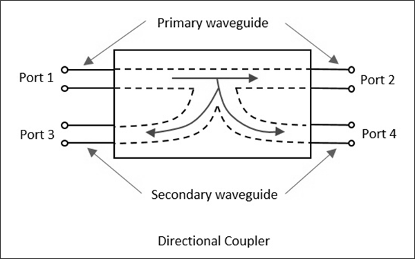
Directional coupler is used to couple the Microwave power which may be unidirectional or bi-directional.
Properties of Directional Couplers
The properties of an ideal directional coupler are as follows.
All the terminations are matched to the ports.
When the power travels from Port 1 to Port 2, some portion of it gets coupled to Port 4 but not to Port 3.
As it is also a bi-directional coupler, when the power travels from Port 2 to Port 1, some portion of it gets coupled to Port 3 but not to Port 4.
If the power is incident through Port 3, a portion of it is coupled to Port 2, but not to Port 1.
If the power is incident through Port 4, a portion of it is coupled to Port 1, but not to Port 2.
Port 1 and 3 are decoupled as are Port 2 and Port 4.
Ideally, the output of Port 3 should be zero. However, practically, a small amount of power called back power is observed at Port 3. The following figure indicates the power flow in a directional coupler.
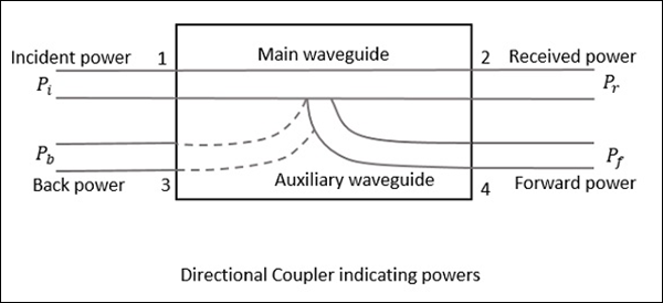
Where
$P_i$ = Incident power at Port 1
$P_r$ = Received power at Port 2
$P_f$ = Forward coupled power at Port 4
$P_b$ = Back power at Port 3
Following are the parameters used to define the performance of a directional coupler.
Coupling Factor (C)
The Coupling factor of a directional coupler is the ratio of incident power to the forward power, measured in dB.
$$C = 10 \: log_{10}\frac{P_i}{P_f}dB$$
Directivity (D)
The Directivity of a directional coupler is the ratio of forward power to the back power, measured in dB.
$$D = 10 \: log_{10}\frac{P_f}{P_b}dB$$
Isolation
It defines the directive properties of a directional coupler. It is the ratio of incident power to the back power, measured in dB.
$$I = 10 \: log_{10}\frac{P_i}{P_b}dB$$
Isolation in dB = Coupling factor + Directivity
Two-Hole Directional Coupler
This is a directional coupler with same main and auxiliary waveguides, but with two small holes that are common between them. These holes are ${\lambda_g}/{4}$ distance apart where λg is the guide wavelength. The following figure shows the image of a two-hole directional coupler.
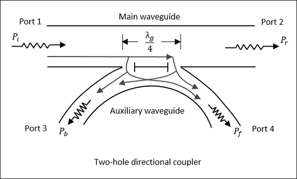
A two-hole directional coupler is designed to meet the ideal requirement of directional coupler, which is to avoid back power. Some of the power while travelling between Port 1 and Port 2, escapes through the holes 1 and 2.
The magnitude of the power depends upon the dimensions of the holes. This leakage power at both the holes are in phase at hole 2, adding up the power contributing to the forward power Pf. However, it is out of phase at hole 1, cancelling each other and preventing the back power to occur.
Hence, the directivity of a directional coupler improves.
Waveguide Joints
As a waveguide system cannot be built in a single piece always, sometimes it is necessary to join different waveguides. This joining must be carefully done to prevent problems such as − Reflection effects, creation of standing waves, and increasing the attenuation, etc.
The waveguide joints besides avoiding irregularities, should also take care of E and H field patterns by not affecting them. There are many types of waveguide joints such as bolted flange, flange joint, choke joint, etc.
Microwave Engineering - Cavity Klystron
For the generation and amplification of Microwaves, there is a need of some special tubes called as Microwave tubes. Of them all, Klystron is an important one.
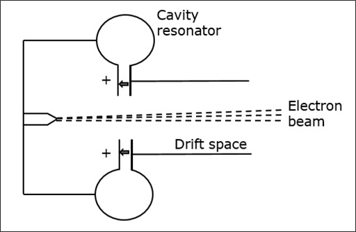
The essential elements of Klystron are electron beams and cavity resonators. Electron beams are produced from a source and the cavity klystrons are employed to amplify the signals. A collector is present at the end to collect the electrons. The whole set up is as shown in the following figure.
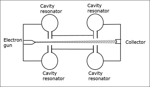
The electrons emitted by the cathode are accelerated towards the first resonator. The collector at the end is at the same potential as the resonator. Hence, usually the electrons have a constant speed in the gap between the cavity resonators.
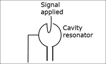
Initially, the first cavity resonator is supplied with a weak high frequency signal, which has to be amplified. The signal will initiate an electromagnetic field inside the cavity. This signal is passed through a coaxial cable as shown in the following figure.
Due to this field, the electrons that pass through the cavity resonator are modulated. On arriving at the second resonator, the electrons are induced with another EMF at the same frequency. This field is strong enough to extract a large signal from the second cavity.
Cavity Resonator
First let us try to understand the constructional details and the working of a cavity resonator. The following figure indicates the cavity resonator.
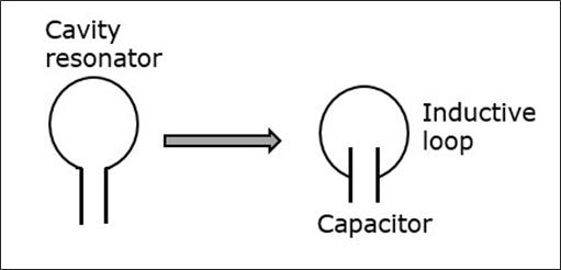
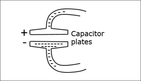
A simple resonant circuit which consists of a capacitor and an inductive loop can be compared with this cavity resonator. A conductor has free electrons. If a charge is applied to the capacitor to get it charged to a voltage of this polarity, many electrons are removed from the upper plate and introduced into the lower plate.
The plate that has more electron deposition will be the cathode and the plate which has lesser number of electrons becomes the anode. The following figure shows the charge deposition on the capacitor.
The electric field lines are directed from the positive charge towards the negative. If the capacitor is charged with reverse polarity, then the direction of the field is also reversed. The displacement of electrons in the tube, constitutes an alternating current. This alternating current gives rise to alternating magnetic field, which is out of phase with the electric field of the capacitor.
When the magnetic field is at its maximum strength, the electric field is zero and after a while, the electric field becomes maximum while the magnetic field is at zero. This exchange of strength happens for a cycle.
Closed Resonator
The smaller the value of the capacitor and the inductivity of the loop, the higher will be the oscillation or the resonant frequency. As the inductance of the loop is very small, high frequency can be obtained.
To produce higher frequency signal, the inductance can be further reduced by placing more inductive loops in parallel as shown in the following figure. This results in the formation of a closed resonator having very high frequencies.
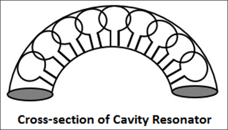
In a closed resonator, the electric and magnetic fields are confined to the interior of the cavity. The first resonator of the cavity is excited by the external signal to be amplified. This signal must have a frequency at which the cavity can resonate. The current in this coaxial cable sets up a magnetic field, by which an electric field originates.
Working of Klystron
To understand the modulation of the electron beam, entering the first cavity, let's consider the electric field. The electric field on the resonator keeps on changing its direction of the induced field. Depending on this, the electrons coming out of the electron gun, get their pace controlled.
As the electrons are negatively charged, they are accelerated if moved opposite to the direction of the electric field. Also, if the electrons move in the same direction of the electric field, they get decelerated. This electric field keeps on changing, therefore the electrons are accelerated and decelerated depending upon the change of the field. The following figure indicates the electron flow when the field is in the opposite direction.
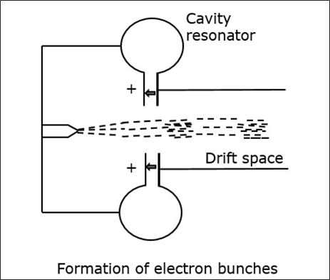
While moving, these electrons enter the field free space called as the drift space between the resonators with varying speeds, which create electron bunches. These bunches are created due to the variation in the speed of travel.
These bunches enter the second resonator, with a frequency corresponding to the frequency at which the first resonator oscillates. As all the cavity resonators are identical, the movement of electrons makes the second resonator to oscillate. The following figure shows the formation of electron bunches.
The induced magnetic field in the second resonator induces some current in the coaxial cable, initiating the output signal. The kinetic energy of the electrons in the second cavity is almost equal to the ones in the first cavity and so no energy is taken from the cavity.
The electrons while passing through the second cavity, few of them are accelerated while bunches of electrons are decelerated. Hence, all the kinetic energy is converted into electromagnetic energy to produce the output signal.
Amplification of such two-cavity Klystron is low and hence multi-cavity Klystrons are used.
The following figure depicts an example of multi-cavity Klystron amplifier.
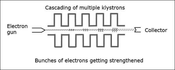
With the signal applied in the first cavity, we get weak bunches in the second cavity. These will set up a field in the third cavity, which produces more concentrated bunches and so on. Hence, the amplification is larger.
Microwave Engineering - Reflex Klystron
This microwave generator, is a Klystron that works on reflections and oscillations in a single cavity, which has a variable frequency.
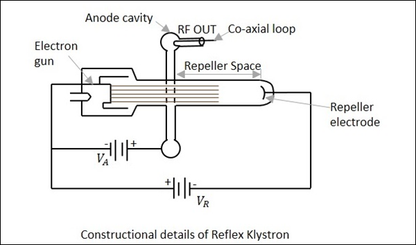
Reflex Klystron consists of an electron gun, a cathode filament, an anode cavity, and an electrode at the cathode potential. It provides low power and has low efficiency.
Construction of Reflex Klystron
The electron gun emits the electron beam, which passes through the gap in the anode cavity. These electrons travel towards the Repeller electrode, which is at high negative potential. Due to the high negative field, the electrons repel back to the anode cavity. In their return journey, the electrons give more energy to the gap and these oscillations are sustained. The constructional details of this reflex klystron is as shown in the following figure.
It is assumed that oscillations already exist in the tube and they are sustained by its operation. The electrons while passing through the anode cavity, gain some velocity.
Operation of Reflex Klystron
The operation of Reflex Klystron is understood by some assumptions. The electron beam is accelerated towards the anode cavity.
Let us assume that a reference electron er crosses the anode cavity but has no extra velocity and it repels back after reaching the Repeller electrode, with the same velocity. Another electron, let's say ee which has started earlier than this reference electron, reaches the Repeller first, but returns slowly, reaching at the same time as the reference electron.
We have another electron, the late electron el, which starts later than both er and ee, however, it moves with greater velocity while returning back, reaching at the same time as er and ee.
Now, these three electrons, namely er, ee and el reach the gap at the same time, forming an electron bunch. This travel time is called as transit time, which should have an optimum value. The following figure illustrates this.
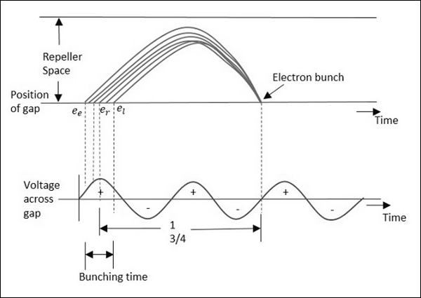
The anode cavity accelerates the electrons while going and gains their energy by retarding them during the return journey. When the gap voltage is at maximum positive, this lets the maximum negative electrons to retard.
The optimum transit time is represented as
$$T = n + \frac{3}{4} \quad where \: n \: is \:an \:integer$$
This transit time depends upon the Repeller and anode voltages.
Applications of Reflex Klystron
Reflex Klystron is used in applications where variable frequency is desirable, such as −
- Radio receivers
- Portable microwave links
- Parametric amplifiers
- Local oscillators of microwave receivers
- As a signal source where variable frequency is desirable in microwave generators.
Travelling Wave Tube
Travelling wave tubes are broadband microwave devices which have no cavity resonators like Klystrons. Amplification is done through the prolonged interaction between an electron beam and Radio Frequency (RF) field.
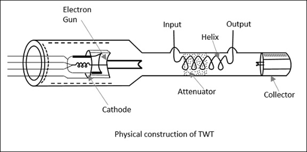
Construction of Travelling Wave Tube
Travelling wave tube is a cylindrical structure which contains an electron gun from a cathode tube. It has anode plates, helix and a collector. RF input is sent to one end of the helix and the output is drawn from the other end of the helix.
An electron gun focusses an electron beam with the velocity of light. A magnetic field guides the beam to focus, without scattering. The RF field also propagates with the velocity of light which is retarded by a helix. Helix acts as a slow wave structure. Applied RF field propagated in helix, produces an electric field at the center of the helix.
The resultant electric field due to applied RF signal, travels with the velocity of light multiplied by the ratio of helix pitch to helix circumference. The velocity of electron beam, travelling through the helix, induces energy to the RF waves on the helix.
The following figure explains the constructional features of a travelling wave tube.
Thus, the amplified output is obtained at the output of TWT. The axial phase velocity $V_p$ is represented as
$$V_p = V_c \left ( {Pitch}/{2\pi r} \right )$$
Where r is the radius of the helix. As the helix provides least change in $V_p$ phase velocity, it is preferred over other slow wave structures for TWT. In TWT, the electron gun focuses the electron beam, in the gap between the anode plates, to the helix, which is then collected at the collector. The following figure explains the electrode arrangements in a travelling wave tube.
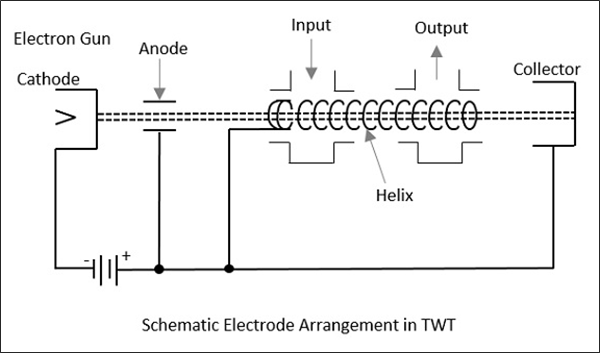
Operation of Travelling Wave Tube
The anode plates, when at zero potential, which means when the axial electric field is at a node, the electron beam velocity remains unaffected. When the wave on the axial electric field is at positive antinode, the electron from the electron beam moves in the opposite direction. This electron being accelerated, tries to catch up with the late electron, which encounters the node of the RF axial field.
At the point, where the RF axial field is at negative antinode, the electron referred earlier, tries to overtake due to the negative field effect. The electrons receive modulated velocity. As a cumulative result, a second wave is induced in the helix. The output becomes larger than the input and results in amplification.
Applications of Travelling Wave Tube
There are many applications of a travelling wave tube.
TWT is used in microwave receivers as a low noise RF amplifier.
TWTs are also used in wide-band communication links and co-axial cables as repeater amplifiers or intermediate amplifiers to amplify low signals.
TWTs have a long tube life, due to which they are used as power output tubes in communication satellites.
Continuous wave high power TWTs are used in Troposcatter links, because of large power and large bandwidths, to scatter to large distances.
TWTs are used in high power pulsed radars and ground based radars.
Microwave Engineering - Magnetrons
Unlike the tubes discussed so far, Magnetrons are the cross-field tubes in which the electric and magnetic fields cross, i.e. run perpendicular to each other. In TWT, it was observed that electrons when made to interact with RF, for a longer time, than in Klystron, resulted in higher efficiency. The same technique is followed in Magnetrons.
Types of Magnetrons
There are three main types of Magnetrons.
Negative Resistance Type
- The negative resistance between two anode segments, is used.
- They have low efficiency.
- They are used at low frequencies (< 500 MHz).
Cyclotron Frequency Magnetrons
The synchronism between the electric component and oscillating electrons is considered.
Useful for frequencies higher than 100MHz.
Travelling Wave or Cavity Type
The interaction between electrons and rotating EM field is taken into account.
High peak power oscillations are provided.
Useful in radar applications.
Cavity Magnetron
The Magnetron is called as Cavity Magnetron because the anode is made into resonant cavities and a permanent magnet is used to produce a strong magnetic field, where the action of both of these make the device work.
Construction of Cavity Magnetron
A thick cylindrical cathode is present at the center and a cylindrical block of copper, is fixed axially, which acts as an anode. This anode block is made of a number of slots that acts as resonant anode cavities.
The space present between the anode and cathode is called as Interaction space. The electric field is present radially while the magnetic field is present axially in the cavity magnetron. This magnetic field is produced by a permanent magnet, which is placed such that the magnetic lines are parallel to cathode and perpendicular to the electric field present between the anode and the cathode.
The following figures show the constructional details of a cavity magnetron and the magnetic lines of flux present, axially.
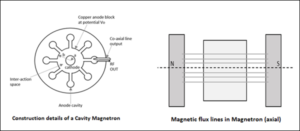
This Cavity Magnetron has 8 cavities tightly coupled to each other. An N-cavity magnetron has $N$ modes of operations. These operations depend upon the frequency and the phase of oscillations. The total phase shift around the ring of this cavity resonators should be $2n\pi$ where $n$ is an integer.
If $\phi_v$ represents the relative phase change of the AC electric field across adjacent cavities, then
$$\phi_v = \frac{2 \pi n}{N}$$
Where $n = 0, \: \pm1,\: \pm2,\: \pm \: (\frac{N}{2} -1), \: \pm \frac{N}{2}$
Which means that $\frac{N}{2}$ mode of resonance can exist if $N$ is an even number.
If,
$$n = \frac{N}{2} \quad then \quad \phi_v = \pi$$
This mode of resonance is called as $\pi-mode$.
$$n = 0 \quad then \quad \phi_v = 0$$
This is called as the Zero mode, because there will be no RF electric field between the anode and the cathode. This is also called as Fringing Field and this mode is not used in magnetrons.
Operation of Cavity Magnetron
When the Cavity Klystron is under operation, we have different cases to consider. Let us go through them in detail.
Case 1
If the magnetic field is absent, i.e. B = 0, then the behavior of electrons can be observed in the following figure. Considering an example, where electron a directly goes to anode under radial electric force.
Case 2
If there is an increase in the magnetic field, a lateral force acts on the electrons. This can be observed in the following figure, considering electron b which takes a curved path, while both forces are acting on it.
Radius of this path is calculated as
$$R = \frac{mv}{eB}$$
It varies proportionally with the velocity of the electron and it is inversely proportional to the magnetic field strength.
Case 3
If the magnetic field B is further increased, the electron follows a path such as the electron c, just grazing the anode surface and making the anode current zero. This is called as "Critical magnetic field" $(B_c)$, which is the cut-off magnetic field. Refer the following figure for better understanding.
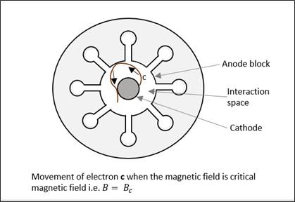
Case 4
If the magnetic field is made greater than the critical field,
$$B > B_c$$
Then the electrons follow a path as electron d, where the electron jumps back to the cathode, without going to the anode. This causes "back heating" of the cathode. Refer the following figure.
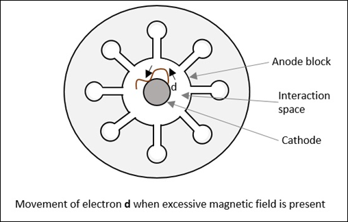
This is achieved by cutting off the electric supply once the oscillation begins. If this is continued, the emitting efficiency of the cathode gets affected.
Operation of Cavity Magnetron with Active RF Field
We have discussed so far the operation of cavity magnetron where the RF field is absent in the cavities of the magnetron (static case). Let us now discuss its operation when we have an active RF field.
As in TWT, let us assume that initial RF oscillations are present, due to some noise transient. The oscillations are sustained by the operation of the device. There are three kinds of electrons emitted in this process, whose actions are understood as electrons a, b and c, in three different cases.
Case 1
When oscillations are present, an electron a, slows down transferring energy to oscillate. Such electrons that transfer their energy to the oscillations are called as favored electrons. These electrons are responsible for bunching effect.
Case 2
In this case, another electron, say b, takes energy from the oscillations and increases its velocity. As and when this is done,
- It bends more sharply.
- It spends little time in interaction space.
- It returns to the cathode.
These electrons are called as unfavored electrons. They don't participate in the bunching effect. Also, these electrons are harmful as they cause "back heating".
Case 3
In this case, electron c, which is emitted a little later, moves faster. It tries to catch up with electron a. The next emitted electron d, tries to step with a. As a result, the favored electrons a, c and d form electron bunches or electron clouds. It called as "Phase focusing effect".
This whole process is understood better by taking a look at the following figure.
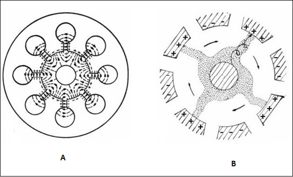
Figure A shows the electron movements in different cases while figure B shows the electron clouds formed. These electron clouds occur while the device is in operation. The charges present on the internal surface of these anode segments, follow the oscillations in the cavities. This creates an electric field rotating clockwise, which can be actually seen while performing a practical experiment.
While the electric field is rotating, the magnetic flux lines are formed in parallel to the cathode, under whose combined effect, the electron bunches are formed with four spokes, directed in regular intervals, to the nearest positive anode segment, in spiral trajectories.
Measurement Devices
Among the Microwave measurement devices, a setup of Microwave bench, which consists of Microwave devices has a prominent place. This whole setup, with few alternations, is able to measure many values like guide wavelength, free space wavelength, cut-off wavelength, impedance, frequency, VSWR, Klystron characteristics, Gunn diode characteristics, power measurements, etc.
The output produced by microwaves, in determining power is generally of a little value. They vary with the position in a transmission line. There should be an equipment to measure the Microwave power, which in general will be a Microwave bench setup.
Microwave Bench General Measurement Setup
This setup is a combination of different parts which can be observed in detail. The following figure clearly explains the setup.
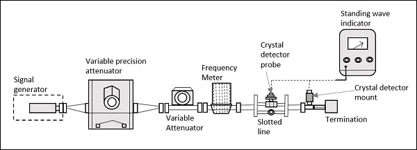
Signal Generator
As the name implies, it generates a microwave signal, in the order of a few milliwatts. This uses velocity modulation technique to transfer continuous wave beam into milliwatt power.
A Gunn diode oscillator or a Reflex Klystron tube could be an example for this microwave signal generator.
Precision Attenuator
This is the attenuator which selects the desired frequency and confines the output around 0 to 50db. This is variable and can be adjusted according to the requirement.
Variable Attenuator
This attenuator sets the amount of attenuation. It can be understood as a fine adjustment of values, where the readings are checked against the values of Precision Attenuator.
Isolator
This removes the signal that is not required to reach the detector mount. Isolator allows the signal to pass through the waveguide only in one direction.
Frequency Meter
This is the device which measures the frequency of the signal. With this frequency meter, the signal can be adjusted to its resonance frequency. It also gives provision to couple the signal to waveguide.
Crystal Detector
A crystal detector probe and crystal detector mount are indicated in the above figure, where the detector is connected through a probe to the mount. This is used to demodulate the signals.
Standing Wave Indicator
The standing wave voltmeter provides the reading of standing wave ratio in dB. The waveguide is slotted by some gap to adjust the clock cycles of the signal. Signals transmitted by waveguide are forwarded through BNC cable to VSWR or CRO to measure its characteristics.
A microwave bench set up in real-time application would look as follows −
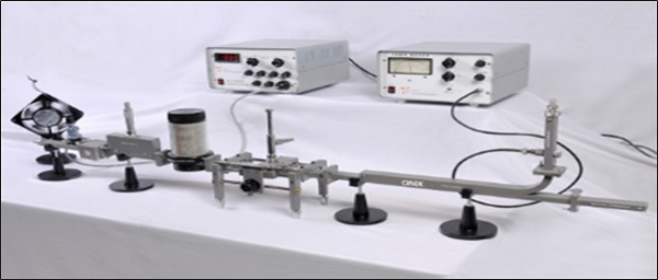
Now, let us take a look at the important part of this microwave bench, the slotted line.
Slotted Line
In a microwave transmission line or waveguide, the electromagnetic field is considered as the sum of incident wave from the generator and the reflected wave to the generator. The reflections indicate a mismatch or a discontinuity. The magnitude and phase of the reflected wave depends upon the amplitude and phase of the reflecting impedance.
The standing waves obtained are measured to know the transmission line imperfections which is necessary to have a knowledge on impedance mismatch for effective transmission. This slotted line helps in measuring the standing wave ratio of a microwave device.
Construction
The slotted line consists of a slotted section of a transmission line, where the measurement has to be done. It has a travelling probe carriage, to let the probe get connected wherever necessary, and the facility for attaching and detecting the instrument.
In a waveguide, a slot is made at the center of the broad side, axially. A movable probe connected to a crystal detector is inserted into the slot of the waveguide.
Operation
The output of the crystal detector is proportional to the square of the input voltage applied. The movable probe permits convenient and accurate measurement at its position. But, as the probe is moved along, its output is proportional to the standing wave pattern, which is formed inside the waveguide. A variable attenuator is employed here to obtain accurate results.
The output VSWR can be obtained by
$$VSWR = \sqrt{\frac{V_{max}}{V_{min}}}$$
Where, $V$ is the output voltage.
The following figure shows the different parts of a slotted line labelled.
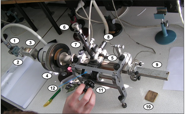
The parts labelled in the above figure indicate the following.
- Launcher − Invites the signal.
- Smaller section of the waveguide.
- Isolator − Prevents reflections to the source.
- Rotary variable attenuator − For fine adjustments.
- Slotted section − To measure the signal.
- Probe depth adjustment.
- Tuning adjustments − To obtain accuracy.
- Crystal detector − Detects the signal.
- Matched load − Absorbs the power exited.
- Short circuit − Provision to get replaced by a load.
- Rotary knob − To adjust while measuring.
- Vernier gauge − For accurate results.
In order to obtain a low frequency modulated signal on an oscilloscope, a slotted line with a tunable detector is employed. A slotted line carriage with a tunable detector can be used to measure the following.
- VSWR (Voltage Standing Wave Ratio)
- Standing wave pattern
- Impedance
- Reflection coefficient
- Return loss
- Frequency of the generator used
Tunable Detector
The tunable detector is a detector mount which is used to detect the low frequency square wave modulated microwave signals. The following figure gives an idea of a tunable detector mount.
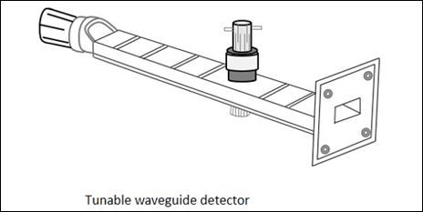
The following image represents the practical application of this device. It is terminated at the end and has an opening at the other end just as the above one.
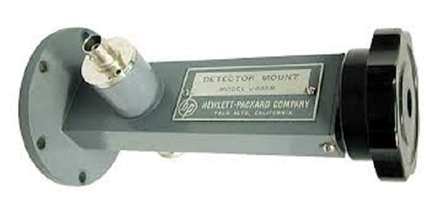
To provide a match between the Microwave transmission system and the detector mount, a tunable stub is often used. There are three different types of tunable stubs.
- Tunable waveguide detector
- Tunable co-axial detector
- Tunable probe detector
Also, there are fixed stubs like −
- Fixed broad band tuned probe
- Fixed waveguide matched detector mount
The detector mount is the final stage on a Microwave bench which is terminated at the end.
Microwave Engineering - Measurements
In the field of Microwave engineering, there occurs many applications, as already stated in first chapter. Hence, while using different applications, we often come across the need of measuring different values such as Power, Attenuation, Phase shift, VSWR, Impedance, etc. for the effective usage.
In this chapter, let us take a look at the different measurement techniques.
Measurement of Power
The Microwave Power measured is the average power at any position in waveguide. Power measurement can be of three types.
-
Measurement of Low power (0.01mW to 10mW)
Example − Bolometric technique
-
Measurement of Medium power (10mW to 1W)
Example − Calorimeter technique
-
Measurement of High power (>10W)
Example − Calorimeter Watt meter
Let us go through them in detail.
Measurement of Low Power
The measurement of Microwave power around 0.01mW to 10mW, can be understood as the measurement of low power.
Bolometer is a device which is used for low Microwave power measurements. The element used in bolometer could be of positive or negative temperature coefficient. For example, a barrater has a positive temperature coefficient whose resistance increases with the increase in temperature. Thermistor has negative temperature coefficient whose resistance decreases with the increase in temperature.
Any of them can be used in the bolometer, but the change in resistance is proportional to Microwave power applied for measurement. This bolometer is used in a bridge of the arms as one so that any imbalance caused, affects the output. A typical example of a bridge circuit using a bolometer is as shown in the following figure.
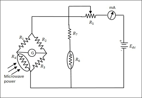
The milliammeter here, gives the value of the current flowing. The battery is variable, which is varied to obtain balance, when an imbalance is caused by the behavior of the bolometer. This adjustment which is made in DC battery voltage is proportional to the Microwave power. The power handling capacity of this circuit is limited.
Measurement of Medium Power
The measurement of Microwave power around 10mW to 1W, can be understood as the measurement of medium power.
A special load is employed, which usually maintains a certain value of specific heat. The power to be measured, is applied at its input which proportionally changes the output temperature of the load that it already maintains. The difference in temperature rise, specifies the input Microwave power to the load.
The bridge balance technique is used here to get the output. The heat transfer method is used for the measurement of power, which is a Calorimetric technique.
Measurement of High Power
The measurement of Microwave power around 10W to 50KW, can be understood as the measurement of high power.
The High Microwave power is normally measured by Calorimetric watt meters, which can be of dry and flow type. The dry type is named so as it uses a coaxial cable which is filled with di-electric of high hysteresis loss, whereas the flow type is named so as it uses water or oil or some liquid which is a good absorber of microwaves.
The change in temperature of the liquid before and after entering the load, is taken for the calibration of values. The limitations in this method are like flow determination, calibration and thermal inertia, etc.
Measurement of Attenuation
In practice, Microwave components and devices often provide some attenuation. The amount of attenuation offered can be measured in two ways. They are − Power ratio method and RF substitution method.
Attenuation is the ratio of input power to the output power and is normally expressed in decibels.
$$Attenuation \: in \: dBs = 10 \: log\frac{P_{in}}{P_{out}}$$
Where $P_{in}$ = Input power and $P_{out}$ = Output power
Power Ratio Method
In this method, the measurement of attenuation takes place in two steps.
Step 1 − The input and output power of the whole Microwave bench is done without the device whose attenuation has to be calculated.
Step 2 − The input and output power of the whole Microwave bench is done with the device whose attenuation has to be calculated.
The ratio of these powers when compared, gives the value of attenuation.
The following figures are the two setups which explain this.
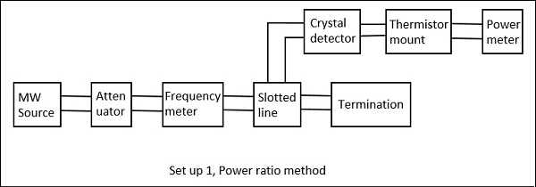
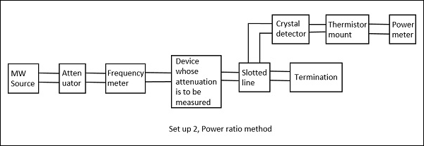
Drawback − The power and the attenuation measurements may not be accurate, when the input power is low and attenuation of the network is large.
RF Substitution Method
In this method, the measurement of attenuation takes place in three steps.
Step 1 − The output power of the whole Microwave bench is measured with the network whose attenuation has to be calculated.
Step 2 − The output power of the whole Microwave bench is measured by replacing the network with a precision calibrated attenuator.
Step 3 − Now, this attenuator is adjusted to obtain the same power as measured with the network.
The following figures are the two setups which explain this.
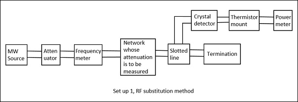
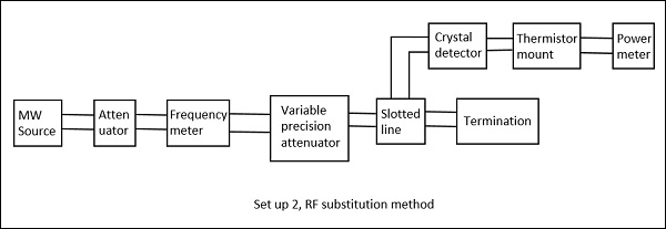
The adjusted value on the attenuator gives the attenuation of the network directly. The drawback in the above method is avoided here and hence this is a better procedure to measure the attenuation.
Measurement of Phase Shift
In practical working conditions, there might occur a phase change in the signal from the actual signal. To measure such phase shift, we use a comparison technique, by which we can calibrate the phase shift.
The setup to calculate the phase shift is shown in the following figure.
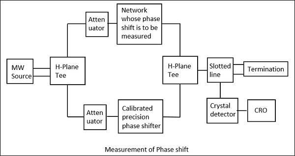
Here, after the microwave source generates the signal, it is passed through an H-plane Tee junction from which one port is connected to the network whose phase shift is to be measured and the other port is connected to an adjustable precision phase shifter.
The demodulated output is a 1 KHz sine wave, which is observed in the CRO connected. This phase shifter is adjusted such that its output of 1 KHz sine wave also matches the above. After the matching is done by observing in the dual mode CRO, this precision phase shifter gives us the reading of phase shift. This is clearly understood by the following figure.
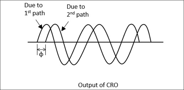
This procedure is the mostly used one in the measurement of phase shift. Now, let us see how to calculate the VSWR.
Measurement of VSWR
In any Microwave practical applications, any kind of impedance mismatches lead to the formation of standing waves. The strength of these standing waves is measured by Voltage Standing Wave Ratio ($VSWR$). The ratio of maximum to minimum voltage gives the $VSWR$, which is denoted by $S$.
$$S = \frac{V_{max}}{V_{min}} = \frac{1+\rho }{1-\rho}$$
Where, $\rho = reflection \: co - efficient = \frac{P_{reflected}}{P_{incident}}$
The measurement of $VSWR$ can be done in two ways, Low $VSWR$ and High $VSWR$ measurements.
Measurement of Low VSWR (S
The measurement of low $VSWR$ can be done by adjusting the attenuator to get a reading on a DC millivoltmeter which is VSWR meter. The readings can be taken by adjusting the slotted line and the attenuator in such a way that the DC millivoltmeter shows a full scale reading as well as a minimum reading.
Now these two readings are calculated to find out the $VSWR$ of the network.
Measurement of High VSWR (S>10)
The measurement of high $VSWR$ whose value is greater than 10 can be measured by a method called the double minimum method. In this method, the reading at the minimum value is taken, and the readings at the half point of minimum value in the crest before and the crest after are also taken. This can be understood by the following figure.
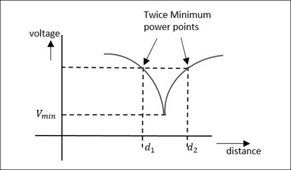
Now, the $VSWR$ can be calculated by a relation, given as −
$$VSWR = \frac{\lambda_{g}}{\pi(d_2-d_1)}$$
Where, $\lambda_g \: is \: the \: guided \: wavelength$
$$\lambda_g = \frac{\lambda_0}{\sqrt{1-(\frac{\lambda_0}{\lambda_c})^2}} \quad where \: \lambda_0 \: = {c}/{f}$$
As the two minimum points are being considered here, this is called as double minimum method. Now, let us learn about the measurement of impedance.
Measurement of Impedance
Apart from Magic Tee, we have two different methods, one is using the slotted line and the other is using the reflectometer.
Impedance Using the Slotted Line
In this method, impedance is measured using slotted line and load $Z_L$ and by using this, $V_{max}$ and $V_{min}$ can be determined. In this method, the measurement of impedance takes place in two steps.
Step 1 − Determining Vmin using load $Z_L$.
Step 2 − Determining Vmin by short circuiting the load.
This is shown in the following figures.
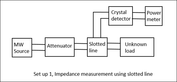
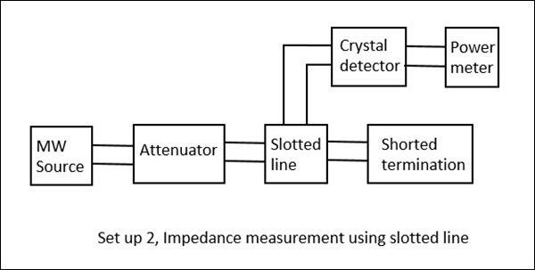
When we try to obtain the values of $V_{max}$ and $V_{min}$ using a load, we get certain values. However, if the same is done by short circuiting the load, the minimum gets shifted, either to the right or to the left. If this shift is to the left, it means that the load is inductive and if it the shift is to the right, it means that the load is capacitive in nature. The following figure explains this.
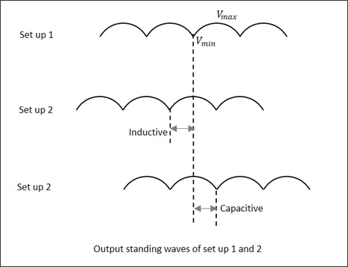
By recording the data, an unknown impedance is calculated. The impedance and reflection coefficient $\rho$ can be obtained in both magnitude and phase.
Impedance Using the Reflectometer
Unlike slotted line, the Reflectometer helps to find only the magnitude of impedance and not the phase angle. In this method, two directional couplers which are identical but differs in direction are taken.
These two couplers are used in sampling the incident power $P_i$ and reflected power $P_r$ from the load. The reflectometer is connected as shown in the following figure. It is used to obtain the magnitude of reflection coefficient $\rho$, from which the impedance can be obtained.
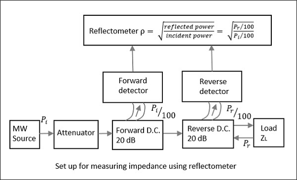
From the reflectometer reading, we have
$$\rho = \sqrt{\frac{P_r}{P_i}}$$
From the value of $\rho$, the $VSWR$, i.e. $S$ and the impedance can be calculated by
$$S = \frac{1+\rho}{1-\rho} \quad and \quad \frac{z-z_g}{z+z_g} = \rho$$
Where, $z_g$ is known wave impedance and $z$ is unknown impedance.
Though the forward and reverse wave parameters are observed here, there will be no interference due to the directional property of the couplers. The attenuator helps in maintaining low input power.
Measurement of Q of Cavity Resonator
Though there are three methods such as Transmission method, Impedance method, and Transient decay or Decrement method for measuring Q of a cavity resonator, the easiest and most followed method is the Transmission Method. Hence, let us take a look at its measurement setup.
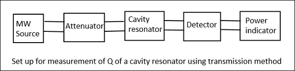
In this method, the cavity resonator acts as the device that transmits. The output signal is plotted as a function of frequency which results in a resonant curve as shown in the following figure.
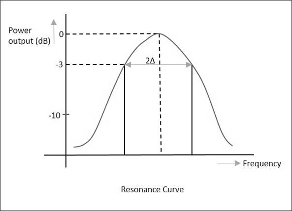
From the setup above, the signal frequency of the microwave source is varied, keeping the signal level constant and then the output power is measured. The cavity resonator is tuned to this frequency, and the signal level and the output power is again noted down to notice the difference.
When the output is plotted, the resonance curve is obtained, from which we can notice the Half Power Bandwidth (HPBW) $(2 \Delta)$ values.
$$2\Delta = \pm \frac{1}{Q_L}$$
Where, $Q_L$ is the loaded value
$$or \quad Q_L = \pm \frac{1}{2\Delta} = \pm \frac{w}{2(w-w_0)}$$
If the coupling between the microwave source and the cavity, as well the coupling between the detector and the cavity are neglected, then
$$Q_L = Q_0 \: (unloaded \: Q)$$
Drawback
The main drawback of this system is that, the accuracy is a bit poor in very high Q systems due to narrow band of operation.
We have covered many types of measurement techniques of different parameters. Now, let us try to solve a few example problems on these.
Microwave Engineering - Example Problems
In this chapter, let us have some fun by solving a few numerical problems related to microwaves.
Problem 1
A transmission system using a $TE_{10}$ mode waveguide of dimensions $a = 5cm, b = 3cm$ is operating at 10GHz. The distance measured between two minimum power points is 1mm on a slotted line. Calculate the VSWR of the system.
Solution
Given that $f = 10GHz; a = 5cm; b = 3cm$
For $TE_{10}$ mode waveguide,
$$\lambda_c = 2a = 2 \times 5 = 10 cm$$
$$\lambda_0 = \frac{c}{f} = \frac{3\times10^{10}}{10\times10^9} = 3cm$$
$$d_2-d_1 = 1mm = 10^{-1}cm$$
We know
$$\lambda_g = \frac{\lambda_0}{1-({\lambda_0}/{\lambda_c})^2} = \frac{3}{\sqrt{1-({3}/{10})^2}} = 3.144cm$$
For double minimum method VSWR is given by
$$VSWR = \frac{\lambda_g}{\pi(d_2-d_1)} = \frac{3.144}{\pi(1\times10^{-1})} = 10.003 = 10$$
Hence, the VSWR value for the given transmission system is 10.
Problem 2
In a setup for measuring impedance of a reflectometer, what is the reflection coefficient when the outputs of two couplers are 2mw and 0.5mw respectively?
Solution
Given that
$$\frac{P_i}{100} = 2mw \quad and \quad \frac{P_r}{100} = 0.5mw$$
$$P_i = 2 \times 100mw = 200mw$$
$$P_r = 0.5 \times 100mw = 50mw$$
$$\rho = \sqrt{\frac{P_r}{P_i}} = \sqrt{\frac{50mw}{200mw}} = \sqrt{0.25} = 0.5$$
Hence, the reflection coefficient $\rho$ of the given set up is 0.5.
Problem 3
When two identical couplers are used in a waveguide to sample the incident power as 3mw and reflected power as 0.25mw, then find the value of $VSWR$.
Solution
We know that
$$\rho = \sqrt{\frac{P_r}{P_i}} = \sqrt{\frac{0.25}{3}} = \sqrt{0.0833} = 0.288$$
$$VSWR = S = \frac{1+\rho}{1-\rho} = \frac{1+0.288}{1-0.288} = \frac{1.288}{0.712} = 1.80$$
Hence, the $VSWR$ value for the above system is 1.80
Problem 4
Two identical 30dB directional couplers are used to sample incident and reflected power in a waveguide. The value of VSWR is 6 and the output of the coupler sampling incident power is 5mw. What is the value of the reflected power?
Solution
We know that
$$VSWR = S = \frac{1+\rho}{1-\rho} = 6$$
$$(1+\rho) = 6(1-\rho) = 6 - 6\rho$$
$$7\rho = 5$$
$$\rho = \frac{5}{7} = 0.174$$
To get the value of reflected power, we have
$$\rho = \sqrt{\frac{{P_r}/{10^3}}{{P_i}/{10^3}}} = \sqrt{\frac{P_r}{P_i}}$$
$$or \quad \rho^2 = \frac{P_r}{P_i}$$
$$P_r = \rho^2.P_i = (0.714)^2.5 = 0.510 \times 5 = 2.55$$
Hence, the reflected power in this waveguide is 2.55mW.
