- Microwave Engineering - Home
- Introduction
- Transmission Lines
- Modes of Propagation
- Types of Transmission Lines
- Waveguides
- Components
- Avalanche Transit Time Devices
- Microwave Devices
- E-Plane Tee
- H-Plane Tee
- E-H Plane Tee
- Rat-race Junction
- Directional Couplers
- Cavity Klystron
- Reflex Klystron
- Travelling Wave Tube
- Magnetrons
- Measurement Devices
- Measurements
- Example Problems
- Microwave Engineering -Quick Guide
- Microwave Engineering - Resources
- Microwave Engineering - Discussion
Avalanche Transit Time Devices
The process of having a delay between voltage and current, in avalanche together with transit time, through the material is said to be Negative resistance. The devices that helps to make a diode exhibit this property are called as Avalanche transit time devices.
The examples of the devices that come under this category are IMPATT, TRAPATT and BARITT diodes. Let us take a look at each of them, in detail.
IMPATT Diode
This is a high-power semiconductor diode, used in high frequency microwave applications. The full form IMPATT is IMPact ionization Avalanche Transit Time diode.
A voltage gradient when applied to the IMPATT diode, results in a high current. A normal diode will eventually breakdown by this. However, IMPATT diode is developed to withstand all this. A high potential gradient is applied to back bias the diode and hence minority carriers flow across the junction.
Application of a RF AC voltage if superimposed on a high DC voltage, the increased velocity of holes and electrons results in additional holes and electrons by thrashing them out of the crystal structure by Impact ionization. If the original DC field applied was at the threshold of developing this situation, then it leads to the avalanche current multiplication and this process continues. This can be understood by the following figure.
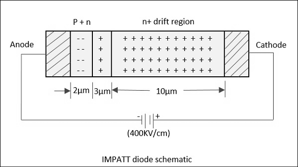
Due to this effect, the current pulse takes a phase shift of 90°. However, instead of being there, it moves towards cathode due to the reverse bias applied. The time taken for the pulse to reach cathode depends upon the thickness of n+ layer, which is adjusted to make it 90° phase shift. Now, a dynamic RF negative resistance is proved to exist. Hence, IMPATT diode acts both as an oscillator and an amplifier.
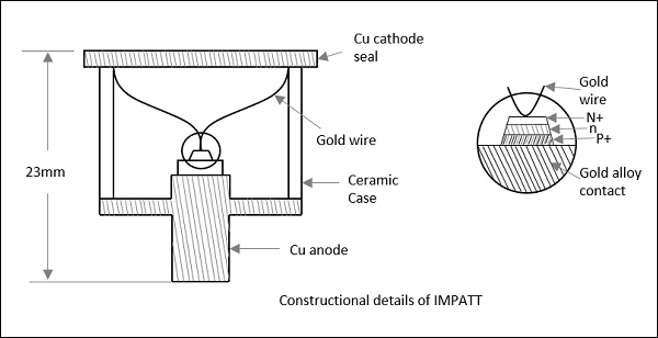
The following figure shows the constructional details of an IMPATT diode.
The efficiency of IMPATT diode is represented as
$$\eta = \left [ \frac{P_{ac}}{P_{dc}} \right ] = \frac{V_a}{V_d}\left [ \frac{I_a}{I_d} \right ]$$
Where,
$P_{ac}$ = AC power
$P_{dc}$ = DC power
$V_a \: \& \: I_a$ = AC voltage & current
$V_d \: \& \: I_d$ = DC voltage & current
Disadvantages
Following are the disadvantages of IMPATT diode.
- It is noisy as avalanche is a noisy process
- Tuning range is not as good as in Gunn diodes
Applications
Following are the applications of IMPATT diode.
- Microwave oscillator
- Microwave generators
- Modulated output oscillator
- Receiver local oscillator
- Negative resistance amplifications
- Intrusion alarm networks (high Q IMPATT)
- Police radar (high Q IMPATT)
- Low power microwave transmitter (high Q IMPATT)
- FM telecom transmitter (low Q IMPATT)
- CW Doppler radar transmitter (low Q IMPATT)
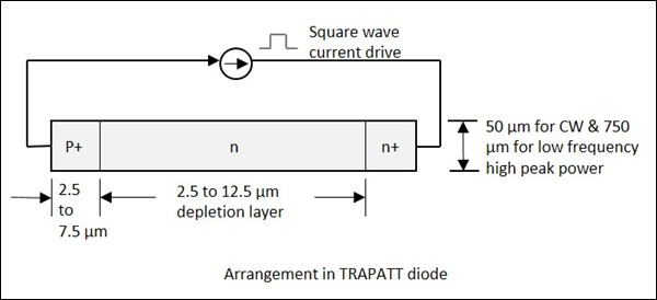
TRAPATT Diode
The full form of TRAPATT diode is TRApped Plasma Avalanche Triggered Transit diode. A microwave generator which operates between hundreds of MHz to GHz. These are high peak power diodes usually n+- p-p+ or p+-n-n+ structures with n-type depletion region, width varying from 2.5 to 1.25 m. The following figure depicts this.
The electrons and holes trapped in low field region behind the zone, are made to fill the depletion region in the diode. This is done by a high field avalanche region which propagates through the diode.
The following figure shows a graph in which AB shows charging, BC shows plasma formation, DE shows plasma extraction, EF shows residual extraction, and FG shows charging.
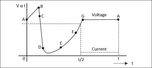
Let us see what happens at each of the points.
A: The voltage at point A is not sufficient for the avalanche breakdown to occur. At A, charge carriers due to thermal generation results in charging of the diode like a linear capacitance.
A-B: At this point, the magnitude of the electric field increases. When a sufficient number of carriers are generated, the electric field is depressed throughout the depletion region causing the voltage to decrease from B to C.
C: This charge helps the avalanche to continue and a dense plasma of electrons and holes is created. The field is further depressed so as not to let the electrons or holes out of the depletion layer, and traps the remaining plasma.
D: The voltage decreases at point D. A long time is required to clear the plasma as the total plasma charge is large compared to the charge per unit time in the external current.
E: At point E, the plasma is removed. Residual charges of holes and electrons remain each at one end of the deflection layer.
E to F: The voltage increases as the residual charge is removed.
F: At point F, all the charge generated internally is removed.
F to G: The diode charges like a capacitor.
G: At point G, the diode current comes to zero for half a period. The voltage remains constant as shown in the graph above. This state continues until the current comes back on and the cycle repeats.
The avalanche zone velocity $V_s$ is represented as
$$V_s = \frac{dx}{dt} = \frac{J}{qN_A}$$
Where
$J$ = Current density
$q$ = Electron charge 1.6 x 10⁻¹⁹
$N_A$ = Doping concentration
The avalanche zone will quickly sweep across most of the diode and the transit time of the carriers is represented as
$$\tau_s = \frac{L}{V_s}$$
Where
$V_s$ = Saturated carrier drift velocity
$L$ = Length of the specimen
The transit time calculated here is the time between the injection and the collection. The repeated action increases the output to make it an amplifier, whereas a microwave low pass filter connected in shunt with the circuit can make it work as an oscillator.
Applications
There are many applications of this diode.
- Low power Doppler radars
- Local oscillator for radars
- Microwave beacon landing system
- Radio altimeter
- Phased array radar, etc.
BARITT Diode
The full form of BARITT Diode is BARrier Injection Transit Time diode. These are the latest invention in this family. Though these diodes have long drift regions like IMPATT diodes, the carrier injection in BARITT diodes is caused by forward biased junctions, but not from the plasma of an avalanche region as in them.
In IMPATT diodes, the carrier injection is quite noisy due to the impact ionization. In BARITT diodes, to avoid the noise, carrier injection is provided by punch through of the depletion region. The negative resistance in a BARITT diode is obtained on account of the drift of the injected holes to the collector end of the diode, made of p-type material.
The following figure shows the constructional details of a BARITT diode.
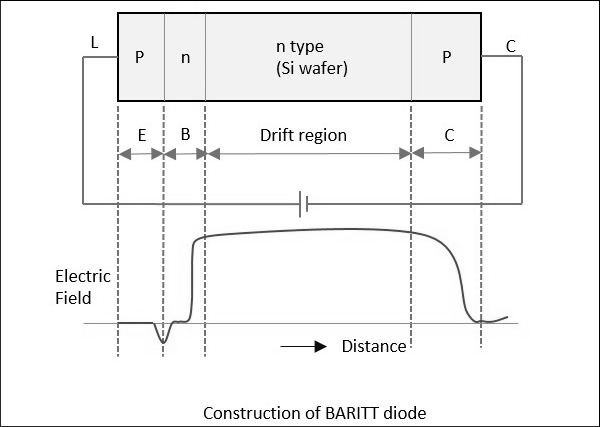
For a m-n-m BARITT diode, Ps-Si Schottky barrier contacts metals with n-type Si wafer in between. A rapid increase in current with applied voltage (above 30v) is due to the thermionic hole injection into the semiconductor.
The critical voltage $(Vc)$ depends on the doping constant $(N)$, length of the semiconductor $(L)$ and the semiconductor dielectric permittivity $(\epsilon S)$ represented as
$$V_c = \frac{qNL^2}{2\epsilon S}$$
Monolithic Microwave Integrated Circuit (MMIC)
Microwave ICs are the best alternative to conventional waveguide or coaxial circuits, as they are low in weight, small in size, highly reliable and reproducible. The basic materials used for monolithic microwave integrated circuits are −
- Substrate material
- Conductor material
- Dielectric films
- Resistive films
These are so chosen to have ideal characteristics and high efficiency. The substrate on which circuit elements are fabricated is important as the dielectric constant of the material should be high with low dissipation factor, along with other ideal characteristics. The substrate materials used are GaAs, Ferrite/garnet, Aluminum, beryllium, glass and rutile.
The conductor material is so chosen to have high conductivity, low temperature coefficient of resistance, good adhesion to substrate and etching, etc. Aluminum, copper, gold, and silver are mainly used as conductor materials. The dielectric materials and resistive materials are so chosen to have low loss and good stability.
Fabrication Technology
In hybrid integrated circuits, the semiconductor devices and passive circuit elements are formed on a dielectric substrate. The passive circuits are either distributed or lumped elements, or a combination of both.
Hybrid integrated circuits are of two types.
- Hybrid IC
- Miniature Hybrid IC
In both the above processes, Hybrid IC uses the distributed circuit elements that are fabricated on IC using a single layer metallization technique, whereas Miniature hybrid IC uses multi-level elements.
Most analog circuits use meso-isolation technology to isolate active n-type areas used for FETs and diodes. Planar circuits are fabricated by implanting ions into semi-insulating substrate, and to provide isolation the areas are masked off.
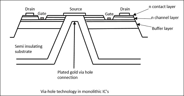
"Via hole" technology is used to connect the source with source electrodes connected to the ground, in a GaAs FET, which is shown in the following figure.
There are many applications of MMICs.
- Military communication
- Radar
- ECM
- Phased array antenna systems
- Spread spectrum and TDMA systems
They are cost-effective and also used in many domestic consumer applications such as DTH, telecom and instrumentation, etc.
