Article Categories
- All Categories
-
 Data Structure
-
 Networking
-
 RDBMS
RDBMS
-
 Operating System
-
 Java
Java
-
 MS Excel
-
 iOS
iOS
-
 HTML
HTML
-
 CSS
CSS
-
 Android
-
 Python
-
 C Programming
-
 C++
C++
-
 C#
C#
-
 MongoDB
-
 MySQL
MySQL
-
 Javascript
-
 PHP
PHP
Memory Read (MR) machine cycle in 8085 Microprocessor
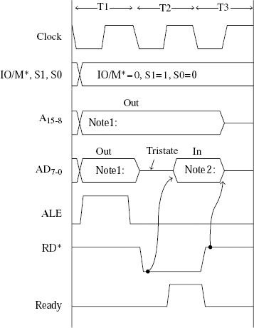
The last three clock cycles in ‘MOV C, M’ instruction are the example for Memory Read machine cycle. Waveforms for Machine Read machine cycle is shown below:

|
Instruction |
Operation |
Address reg. |
|---|---|---|
| LDA 1234H |
Loading W with 12H (or Z with 34H) |
PC |
| POP B |
Popping information from stack top |
SP |
| MOV C, M |
Loading A from memory pointed by HL |
HL |
| LDAX B |
Loading A from memory pointed by BC |
BC |
| LDAX D |
Loading A from memory pointed by DE |
DE |
| LDA 1234H |
Loading A from memory Location 1234H |
WZ |
The data, which is received in a register during a Memory Read machine cycle depends on the MR machine cycle within an instruction as shown below. Where ‘r’ stands for any of the registers A, B, C, D, E, H, or L.
|
Instruction |
Operation |
Data reg. |
|---|---|---|
| MOV r, M |
Loading r from the memory pointer by HL |
R |
| POP PSW |
Loading flags from stack top |
Flags |
| MVI M, 25H |
Loading Temp with 25H from memory |
Temp |
Example
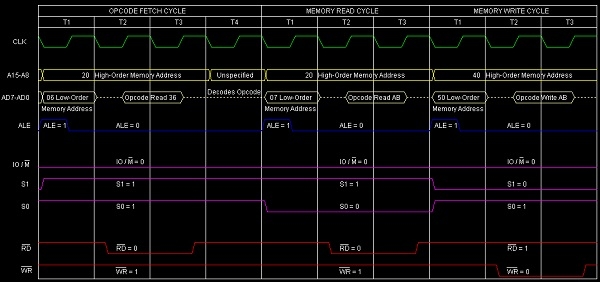
Execution of ‘MVI M, 25H’ instruction. Suppose at location C002H, we have 36H, which is the opcode for the instruction ‘MVI M, ABH’. Here ten clock cycles are needed for the OF, decode, and performing the execution. The first four cycles of the clock constitute the OF machine cycle, and the next three cycles of the clock will be Memory Read machine cycle, and the last three clock cycles will be Memory Write machine cycle.
In addition to the information of the address, the status signals as shown in the following which are activated by the control unit during T1.
ALE = 1, indicates the address present on AD7-0;
IO/M* = 0, indicates that the address is only specified for the memory;
S1 = 0, S0 = 1, indicates that it is MW machine cycle.
Here is the detailing of the instruction execution –
In 8085 Instruction set, this instruction MVI M, d8 is used to load a memory location pointed by HL pair with an 8-bit value directly. This instruction uses immediate addressing for specifying the data. It occupies 2-Bytes in memory.
|
Mnemonics, Operand |
Opcode (in HEX) |
Bytes |
|---|---|---|
| MVI M, Data |
36 |
2 |
As an example, we can consider MVI M, ABH as an example instruction of this type. It is a 2-Byte instruction, with opcode for MVI M using up one Byte, and ABH using up another more Byte. We are considering that HL register pair is containing 16-bit address 4050H and content of that address initially CDH. So after execution of the instruction the updated values will be -
| |
Before |
After |
|---|---|---|
|
(HL) |
(4050) |
(4050) |
|
(4050) |
CDH |
ABH |
Table is shown below
|
Address |
Hex Codes |
Mnemonic |
Comment |
|---|---|---|---|
| 2006 |
36 |
MOV M, ABH |
Content of the memory location pointer by HL register pair will get updated by ABH |
| 2007 |
AB |
|
Operand ABH |
Let us check the timing diagram of this instruction MVI M, ABH

Summary: So this instruction MVI M, ABH requires 2-Bytes, 3-Machine Cycles (Opcode Fetch, Memory Read, Memory Write) and 10 T-States for execution as shown in the timing diagram.


