
Article Categories
- All Categories
-
 Data Structure
-
 Networking
-
 RDBMS
RDBMS
-
 Operating System
-
 Java
Java
-
 MS Excel
-
 iOS
iOS
-
 HTML
HTML
-
 CSS
CSS
-
 Android
-
 Python
-
 C Programming
-
 C++
C++
-
 C#
C#
-
 MongoDB
-
 MySQL
MySQL
-
 Javascript
-
 PHP
PHP
-
 Economics & Finance
I/O Write (IOW) machine cycle in 8085 Microprocessor
The last three clock cycles in the OUT 25H instruction is an example for IOW machine cycle. Waveforms for IOW machine cycle are shown in the figure below:
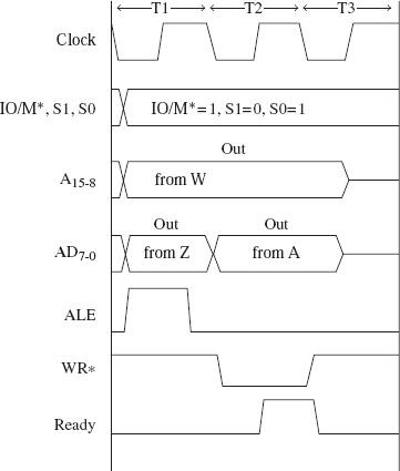
The point to be noted that in an IOW machine cycle, Wand Z registers have identical 8-bit port address. There is also a definite advantage because of address duplication on the addresses ranging from A15-8 and AD7-0 when we are using 8755 (2K × 8 EPROM and two 8-bit ports) and 8155 which is a combination of 256 × 8 RAM, 3 Input Output ports, and 14-bit timer. We can form a 8085-based microcomputer by using only these two chips in addition to 8085 processor. Moreover, these chips do not favor in these days, except when the minimum chip microcomputer configuration is desired for usage.
The 16-bit value in register pair WZ are sent out as the address in the IOW machine cycle. Also the point to be noted that in an IOW machine cycle, only the contents of the Accumulator are sent out as the data to the addressed output port. In 8085, we come across IOW machine cycle only during the execution process of OUT a8 instruction.
Example: In 8085 Instruction set, OUT is a mnemonic that stands for OUTput Accumulator contents to an output port whose 8-bit address is indicated in the instruction as a8. It occupies 2 Bytes in the memory. First Byte specifies the opcode, and the next Byte provides the 8-bit port address.
|
Mnemonics, Operand |
Opcode (in HEX) |
Bytes |
|---|---|---|
| OUT Port-Address |
D3 |
2 |
OUT F0H is an example instruction of this type. The result of execution of this instruction is shown below with an example.
| |
Before |
After |
|---|---|---|
|
(A) |
ABH |
ABH |
|
Output Port F0H |
Any Value |
ABH |
OUT instruction is the only instruction using which Accumulator contents can be sent out to an output port. A possible chip select circuit to connect an output port with an address as F0H is as shown in the followingFig.
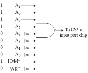
Here as the port address is F0H so the bits ranging from A7 to A0 should have the bit pattern
A7 A6 A5 A4 A3 A2 A1 A0 = 1 1 1 1 0 0 0 0, with WR* = 0, and IO/M* = 1
All these bits will pass through a NAND Gate to product the output logic 1 as Chip-Select (CS), and so the output port chip gets selected. Thus, the chip responds when the 8085 sends out address as F0H, IO/M* as 1, and WR* as 0. In other words, we consider that it is having the output port number F0H.
Notice that it is possible to have an input port with the address F0H, and an output port with the same address F0H. When the 8085 sends out the address as EFH and IO/M* as 1, only one of them is selected based on the RD* and WR* signal status values. Thus, it is possible to have a total of 256 input ports and a total of 256 output ports.
|
Address |
Hex Codes |
Mnemonic |
Comment |
|---|---|---|---|
| 2000 |
D3 |
OUT F0H |
Accumulator content will be sent to port address F0H |
| 2001 |
F0 |
|
F0H as port address |
The timing diagram against this instruction OUT F0H execution is as follows –
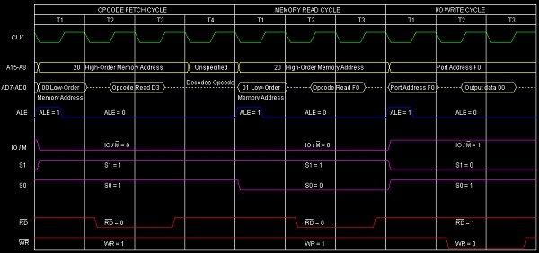
Summary: So this instruction OUT requires 2-Bytes, 3-Machine Cycles (Opcode Fetch, Memory Read, I/O Write) and 10 T-States for execution as shown in the timing diagram.

3K+ Views
