
Article Categories
- All Categories
-
 Data Structure
-
 Networking
-
 RDBMS
RDBMS
-
 Operating System
-
 Java
Java
-
 MS Excel
-
 iOS
iOS
-
 HTML
HTML
-
 CSS
CSS
-
 Android
-
 Python
-
 C Programming
-
 C++
C++
-
 C#
C#
-
 MongoDB
-
 MySQL
MySQL
-
 Javascript
-
 PHP
PHP
-
 Economics & Finance
Read and Write the stack in 8085 Microprocessor
Reading from the Stack
Let us consider that SP contents the address FC78H, and we want to read information from a stack location. In this case, we are not interested in reading from a location whose address is less than the memory address present in SP. This is because 8085 interprets them as useless information. For example, there is no point in reading useless information from memory location FC75H.
SP interprets that, memory locations FC78H, FC79H, ..., FFFFH are all interpreted by 8085 to have useful information. To read from Stack, the instruction is POP in 8085 microprocessor instruction set. Here we shall discuss more about the POP instruction below.
In 8085 Instruction set, with the mnemonic POP, we can pop out 2-Bytes from the top of the stack through rp i.e. register pair e.g. BC, DE, HL or AF. Here AF is a register pair formed with Flag and Accumulator registers and also known as PSW (Processor Status Word). In PSW, Accumulator is the MS Byte, and Flags register is the LS Byte.
|
Mnemonics, Operand |
Opcode (in HEX) |
Bytes |
|---|---|---|
| POP B |
C1 |
1 |
| POP D |
D1 |
1 |
| POP H |
E1 |
1 |
| POP PSW |
F1 |
1 |
In the above mention Opcodes, 2-bits are occupied to mention the register pair. 2-bits can have 4 combinations. So 4 register pairs can be mentioned with POP. As mentioned earlier, they are BC, DE, HL, and AF or PSW.
Note with LXI instruction, we are having 4 possible register pairs can be used i.e. BC, DE, HL, and SP. So at the same time, we can’t have SP and PSW applicable with the same instruction.
|
rp Code |
Register Pair |
|---|---|
| 0 0 |
BC |
| 0 1 |
DE |
| 1 0 |
HL |
| 1 1 |
SP or PSW, but never both at the same time. |
Let us consider the following example for a better understanding of the operation of the instruction.
Here we are considering the instruction POP D which is an instruction falling in the category. As rp can have any of the four values, there are four opcodes for this type of instruction. It occupies only 1-Byte in memory. POP D is an example of instruction of this type. It is 1-Byte instruction. The result of the execution of this instruction is shown below with an example.
|
Before |
After |
|
|---|---|---|
|
(BC) |
AABBH |
AABBH |
|
(SP) |
3FFEH |
4000H |
|
(3FFFH) |
AAH |
AAH |
|
(3FFEH) |
BBH |
BBH |
|
(DE) |
Any value |
AABBH |
|
Address |
Hex Codes |
Mnemonic |
Comment |
|---|---|---|---|
| 2000 |
01 |
LXI B, AABBH |
Initializing BC register pair with AABBH |
| 2001 |
BB |
Low order Byte BBH |
|
| 2002 |
AA |
High order Byte AAH |
|
| 2003 |
31 |
LXI SP,4000H |
Initializing SP with 4000H |
| 2004 |
00 |
Low order Byte 00H |
|
| 2005 |
40 |
High order Byte 40H |
|
| 2006 |
C5 |
PUSH B |
At 3FFFH, AAH and at 3FFEH, BBH will be moved |
| 2007 |
D1 |
POP D |
Popping and initializing DE register pair with stack contents |
The timing diagram against this instruction POP D execution is as follows –
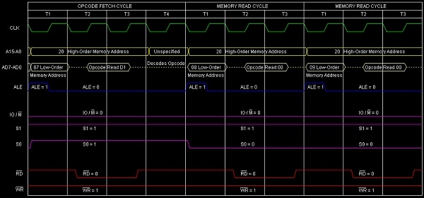
Summary: So this instruction POP requires 1-Byte, 3-Machine Cycles (Opcode Fetch, Memory Read, Memory Read) and 10 T-States for execution as shown in the timing diagram.
Writing to the Stack
Let us consider that SP contents are FC7AH, and we want to write information to a stack location. In this case, we are not interested in writing to a location whose address is equal or greater than the memory address present in SP. This is because the 8085 interprets them as having useful information, which should not be destroyed! For example, there is no point in overwriting and destroying useful information at memory location FD7AH. We should be writing into a location where there is presently useless information, and make it useful.
To write onto Stack, the instruction is PUSH in 8085 microprocessor instruction set. Here we shall discuss more about the PUSH instruction below.
In 8085 Instruction set, PUSH rp instruction stores contents of register pair rp by pushing it into two locations above the top of the stack. rp stands for one of the following register pairs.
rp = BC, DE, HL, or PSW
As rp can have any of the four values, there are four opcodes for this type of instruction. It occupies only 1-Byte in memory.
|
Mnemonics, Operand |
Opcode (in HEX) |
Bytes |
|---|---|---|
| PUSH B |
C5 |
1 |
| PUSH D |
D5 |
1 |
| PUSH H |
E5 |
1 |
| PUSH PSW |
F5 |
1 |
In the above mention Opcodes, 2-bits are occupied to mention the register pair. 2-bits can have 4 combinations. So 4 register pairs can be mentioned with POP. As mentioned earlier, they are BC, DE, HL, and AF or PSW.
Note with LXI instruction, we are having 4 possible register pairs can be used i.e. BC, DE, HL, and SP. So at the same time, we can’t have SP and PSW applicable with the same instruction.
|
rp Code |
Register Pair |
|---|---|
| 0 0 |
BC |
| 0 1 |
DE |
| 1 0 |
HL |
| 1 1 |
SP or PSW, but never both at the same time. |
Let us consider PUSH B as an example of instruction of this category. It is 1-Byte instruction.
The result of the execution of this instruction is shown below with an example.
|
Before |
After |
|
|---|---|---|
|
(BC) |
AABBH |
AABBH |
|
(SP) |
4000H |
3FFEH |
|
(3FFFH) |
Any value |
AAH |
|
(3FFEH) |
Any value |
BBH |
|
Address |
Hex Codes |
Mnemonic |
Comment |
|---|---|---|---|
| 2000 |
01 |
LXI B, AABBH |
Initializing BC register pair with AABBH |
| 2001 |
BB |
Low order Byte BBH |
|
| 2002 |
AA |
High order Byte AAH |
|
| 2003 |
31 |
LXI SP,4000H |
Initializing SP with 4000H |
| 2004 |
00 |
Low order Byte 00H |
|
| 2005 |
40 |
High order Byte 40H |
|
| 2006 |
C5 |
PUSH B |
At 3FFFH, AAH and at 3FFEH, BBH will be moved |
The timing diagram against this instruction PUSH B execution is as follows –
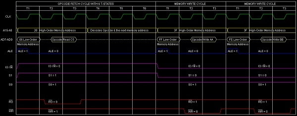
Summary: So this instruction PUSH B requires 1-Byte, 3-Machine Cycles (Opcode Fetch, Memory Write, Memory Write) and 12 T-States for execution as shown in the timing diagram.

2K+ Views
