
Article Categories
- All Categories
-
 Data Structure
-
 Networking
-
 RDBMS
RDBMS
-
 Operating System
-
 Java
Java
-
 MS Excel
-
 iOS
iOS
-
 HTML
HTML
-
 CSS
CSS
-
 Android
-
 Python
-
 C Programming
-
 C++
C++
-
 C#
C#
-
 MongoDB
-
 MySQL
MySQL
-
 Javascript
-
 PHP
PHP
-
 Economics & Finance
I/O Read (IOR) machine cycle in 8085 Microprocessor
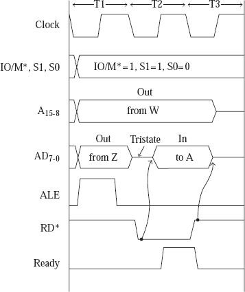
The three clock cycles at the last stages in the IN 35H instruction is an example of machine cycle for IOR. The Waveforms for the IOR machine cycle are shown in the figure below.
The point to be noted that in an IOR machine cycle, Wand Z has identical has port address of 8 bit. The value of 16 bit in the register pair WZ are sent out as the address in an Input Output Read machine cycle. Also the point to be noted that in an IOR machine cycle, only the data is received by the accumulator from the addressed input port. In 8085 processor we come across from the IOR machine cycle just only for the execution process of IN a8 instruction.
Example: In 8085 Instruction set, IN is a mnemonic that stands for INput the Byte from input port’s content to the Accumulator. Input port’s 8-bit address is indicated in the instruction as a8. It occupies 2 Bytes in the memory. First Byte specifies the opcode, and the next Byte provides the 8-bit input port address.
|
Mnemonics, Operand |
Opcode (in HEX) |
Bytes |
|---|---|---|
| IN Port-address |
DB |
2 |
IN F0H is an example instruction of this type. The result of execution of this instruction is shown below with an example.
|
Before |
After |
|
|---|---|---|
|
(A) |
Any Value |
ABH |
|
Input Port F0H |
ABH |
ABH |
IN instruction is the only instruction using which read the input port content to the Accumulator. A possible chip select circuit to connect an input port with an address as F0H is as shown in the followingFig.
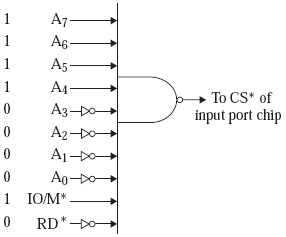
Chip select circuit for input port F0H
Here as the port address is F0H so the bits ranging from A7 to A0 should have the bit pattern
A7 A6 A5 A4 A3 A2 A1 A0 = 1 1 1 1 0 0 0 0, with RD* = 0, and IO/M* = 1
All these bits will pass through a NAND Gate to product the output logic 1 as Chip-Select (CS), and so the input port chip gets selected. Thus, the chip responds when the 8085 sends out address as F0H, IO/M* as 1, and RD* as 0. In other words, we consider that it is having the input port number F0H.
Notice that, it is possible to have an output port with the address F0H, and an input port with the same address F0H. When the 8085 sends out the address as EFH and IO/M* as 1, only one of them is selected based on the RD* and WR* signal status values. Thus, it is possible to have a total of 256 input ports and a total of 256 output ports as well.
|
Address |
Hex Codes |
Mnemonic |
Comment |
|---|---|---|---|
| 2000 |
DB |
IN F0H |
Content from the port address F0H will be written back on to the Accumulator |
| 2001 |
F0 |
F0H as port address |
The timing diagram against this instruction IN F0H execution is as follows –
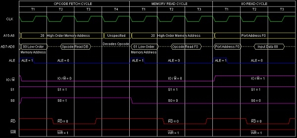
Summary: So this instruction OUT requires 2-Bytes, 3-Machine Cycle (Opcode Fetch, Memory Read, I/O Read) and 10 T-States for execution as shown in the timing diagram.

5K+ Views
